Thin-film piezoelectric element, thin-film piezoelectric actuator, thin-film piezoelectric sensor, hard drive disk, and inkjet printer

a piezoelectric actuator and thin film technology, applied in the direction of generator/motor, inking apparatus, instruments, etc., can solve the problems of increased risk, increased and inapplicability of thin film piezoelectric elements, so as to achieve a higher stable piezoelectric property d31, the effect of reducing the leakage current between the electrode films and further reducing the risk

Active Publication Date: 2014-11-20
TDK CORPARATION
View PDF2 Cites 38 Cited by
  • Summary
  • Abstract
  • Description
  • Claims
  • Application Information

AI Technical Summary

Benefits of technology

[0025]Preferably, in the potassium sodium niobate thin film (KNN thin film) of the thin film piezoelectric element according to the present invention, the region having the largest average crystal grain size M does not lie next to either one of the pair of electrode films. In other words, the region with the largest average crystal grain size M is the region having an average crystal grain size A2. With this structure, the leakage current between the electrode films can be further decreased and a higher stable piezoelectric property −d31 can be obtained.
[0026]In the three regions of the potassium sodium niobate thin film (KNN thin film) in the thin film piezoelectric element according to the present invention, the smallest average crystal grain size m is preferably 60 nm or more and 90 nm or less and the largest average crystal grain size M is preferably 100 nm or more. When a region having an average crystal grain size of 60 nm or more and 90 nm or less lies next to the electrode film, the leakage current between the electrode films can be decreased further. When a region having an average crystal grain size of 100 nm or more is present at the same time, a higher piezoelectric property −d31 can be achieved.
[0027]The potassium sodium niobate thin film (KNN thin film) of the thin film piezoelectric element according to the present invention preferably contains Mn. Incorporation of Mn further decreases the leakage current and a higher piezoelectric property −d31 can be achieved.
[0028]The potassium sodium niobate thin film (KNN thin film) of the thin film piezoelectric element according to the present invention preferably contains three or more elements selected from Li, Sr, Ba, Zr, and Ta. Incorporation of these elements further decreases the leakage current and a higher piezoelectric property −d31 can be achieved.
[0029]With the thin film piezoelectric element according to the present invention, the leakage current can be decreased and the piezoelectric properties can be improved compared to conventional thin film piezoelectric elements that use KNN thin films. The leakage current can be decreased and the piezoelectric properties can be improved also with a thin film piezoelectric actuator and a thin film piezoelectric sensor according to the present invention. Thus, high-performance hard disk drives and ink jet printers can be provided.

Problems solved by technology

However, when the crystal grain size is large and oxygen vacancies occur in the crystal grain boundaries formed in the film thickness direction (a direction perpendicular to an electrode film), the crystal grain boundaries act as passages for an electrical current and there is an increased risk that the leakage current between the electrode films will increase.
Thus, this thin film piezoelectric element is not practically applicable.
However, where dielectric thin films obtained by a sputtering method are concerned, it is difficult to eliminate all oxygen vacancies in the crystal grain boundaries in the films by conducting annealing after film formation, although some effect is achieved by the annealing.
Accordingly, performing annealing after film formation is not sufficient as a countermeasure for decreasing the leakage current between electrode films.

Method used


Image

  • Thin-film piezoelectric element, thin-film piezoelectric actuator, thin-film piezoelectric sensor, hard drive disk, and inkjet printer
  • Thin-film piezoelectric element, thin-film piezoelectric actuator, thin-film piezoelectric sensor, hard drive disk, and inkjet printer
  • Thin-film piezoelectric element, thin-film piezoelectric actuator, thin-film piezoelectric sensor, hard drive disk, and inkjet printer

Examples


example 1

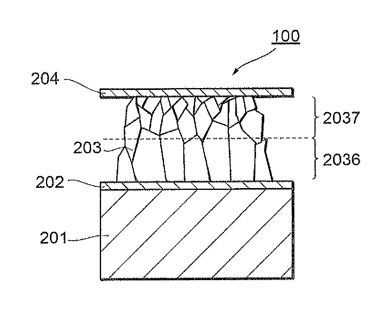
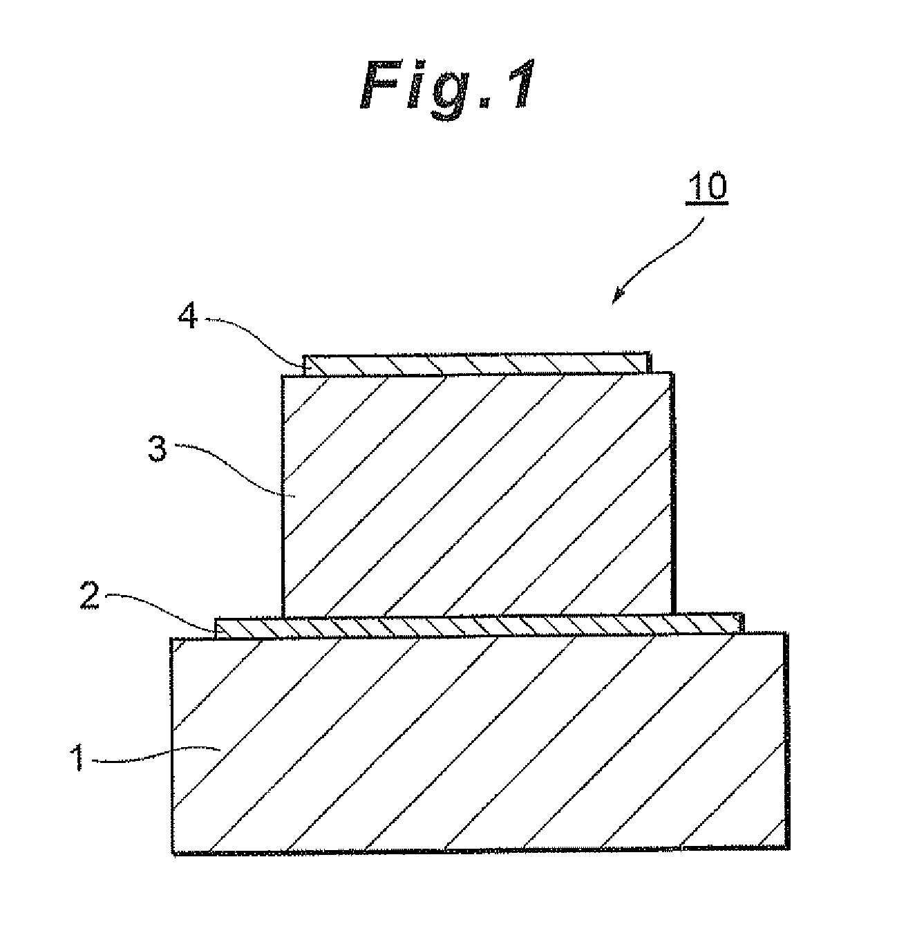
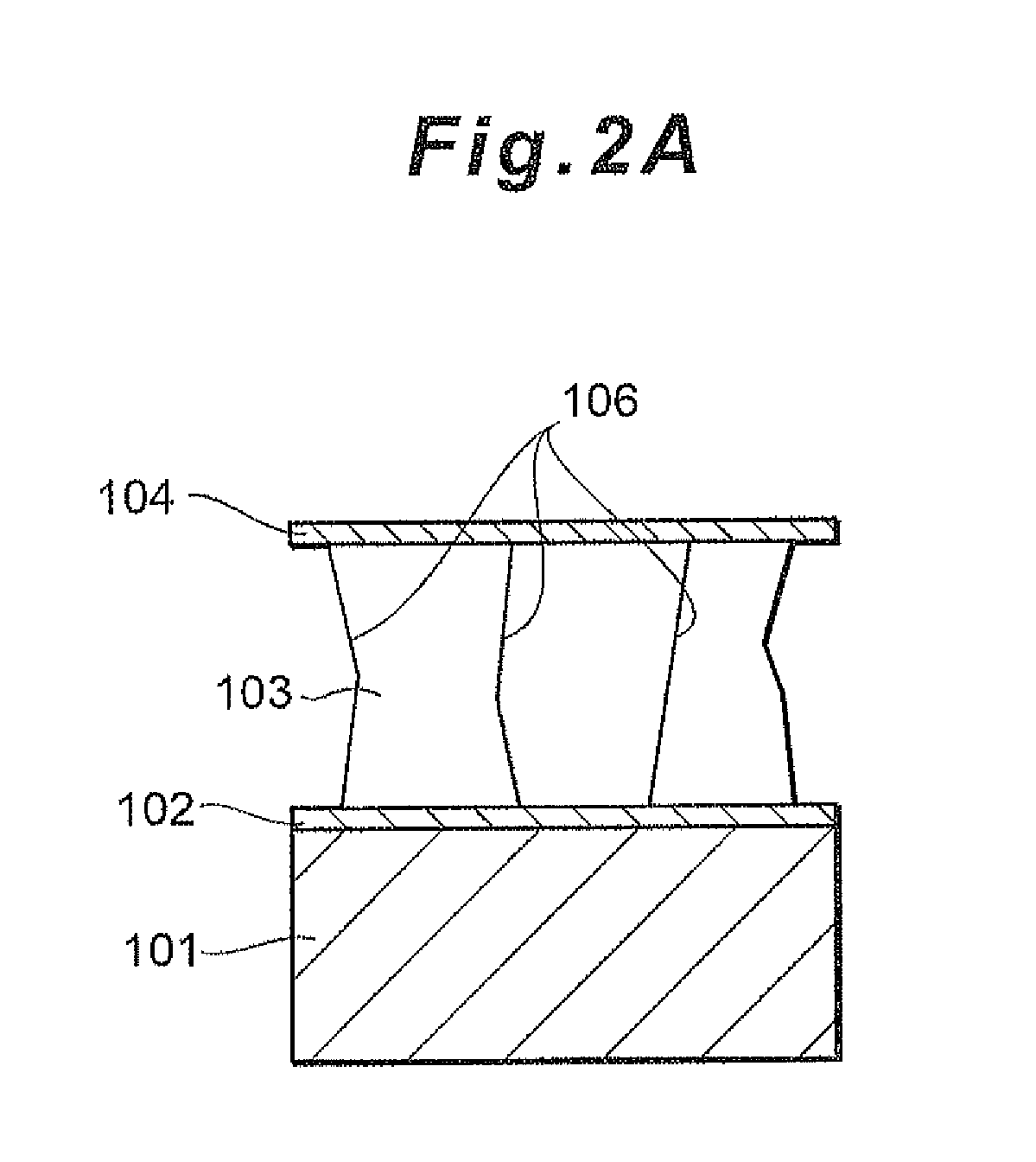
[0112]First, a lower electrode film 2 which serves as a base film of a piezoelectric thin film 3 was formed on a single crystal silicon substrate 1 by crystal growth. This lower electrode film 2 was a Pt film and had a thickness of 200 nm. The method for forming was a sputtering method and the film was formed while setting the temperature of the substrate 1 to 500° C.

[0113]Next, a first layer of a piezoelectric thin film was formed by using a (K,Na)NbO3 sputtering target not containing any additives. The method for forming was a sputtering method and the film was formed while setting the temperature of the substrate 1 to 580° C. The thickness of the piezoelectric thin film under this condition was 0.7 μm. It is known that, in the case where the piezoelectric thin film 3 is a KNN thin film, crystals show the highest c-axis orientation when the temperature of the substrate 1 is set to 550° C.

[0114]Next, a second layer of the piezoelectric thin film was formed while setting the tempera...

examples 9 and 10

[0131]A (K,Na)NbO3 sputtering target to which 0.4 at % of Mn was added was used as a sputtering target for forming the piezoelectric thin film 3. The piezoelectric thin film 3 was formed while the substrate temperature was set as shown in Table 1. The rest of the conditions were the same as in Example 1 and the thin film piezoelectric element 10 was prepared and the properties were evaluated. The preparation conditions and the evaluation results are shown in Table 1.

examples 11 and 12

[0132]A (K,Na)NbO3 sputtering target to which 0.4 at % of Mn, 1.5 at % of Li, 3.0 at % of Sr, 0.1 at % of Ba, 3.0 at % of Zr, and 4 at % of Ta were added was used as a sputtering target for forming the piezoelectric thin film 3. The piezoelectric thin film 3 was formed while the substrate temperature was set as shown in Table 1. The rest of the conditions were the same as in Example 1 and the thin film piezoelectric element 10 was fabricated and the properties were evaluated. The preparation conditions and the evaluation results are shown in Table 1.


PUM

PropertyMeasurementUnit
average crystal grain sizeaaaaaaaaaa

Abstract

A thin film piezoelectric element according to the present invention includes a potassium sodium niobate thin film having a structure in which a plurality of crystal grains are present in a film thickness direction; and a pair of electrode films sandwiching the potassium sodium niobate thin film. When the potassium sodium niobate thin film is divided into three regions of the same thickness in the film thickness direction and average crystal grain sizes A1, A2, and A3 of the respective regions are determined, a ratio m/M of the smallest average crystal grain size m among A1, A2, and A3 to the largest average crystal grain size M among A1, A2, and A3 is 10% to 80%. The region having the smallest average crystal grain size m lies next to one of the pair of electrode films.

Description

BACKGROUND OF INVENTION[0001]1. Field of Invention[0002]The present invention relates to a thin film piezoelectric element that uses a thin film piezoelectric material, a thin film piezoelectric actuator and a thin film piezoelectric sensor that use the thin film piezoelectric element, and a hard disk drive and an ink jet printer that include the thin film piezoelectric actuator.[0003]2. Background Art[0004]With the increasing demand for lead-free piezoelectric materials in recent years, studies on potassium sodium niobate ((K,Na)NbO3 (also referred to as KNN hereinafter)) have been actively pursued. KNN is attracting much attention since it has a relatively high Curie temperature among lead-free piezoelectric materials and offers favorable piezoelectric properties.[0005]Meanwhile, commercialization of piezoelectric elements that use thin film piezoelectric materials instead of bulk piezoelectric materials is progressing. Examples thereof include piezoelectric sensors, such as gyro ...

Claims


Application Information

Patent Timeline
Patent Type & Authority Applications(United States)
IPC IPC(8): H01L41/08H01L41/187
CPCH01L41/1873H01L41/0805G01L9/008G11B5/5552B41J2/161B41J2/1628B41J2/1629B41J2/1631B41J2/1632B41J2/1646B41J2202/03G01C19/5621G01C19/5628G11B5/483H10N30/1051H10N30/8542H10N30/076B41J2/14233
Inventor MAEJIMA, KAZUHIKOAIDA, YASUHIROTANAKA, YOSHITOMOKURACHI, KATSUYUKISAKUMA, HITOSHI
Owner TDK CORPARATION
Why Eureka
Try Eureka