Iron bus bar having copper layer, and method for manufacturing same
a copper layer and iron bus bar technology, applied in the field of bus bars, can solve the problems of increasing the cost of manufacturing a bus bar, and sensitive to foreign copper prices, etc., and achieves excellent electrical conductivity, high strength, durability and strength.
- Summary
- Abstract
- Description
- Claims
- Application Information
AI Technical Summary
Benefits of technology
Problems solved by technology
Method used
Image
Examples
example 1
[0078]A copper target having a purity of 4N and a size of 450×120×6.35 mm and an iron core were provided, and then cleaned at a base pressure of 5.4×10⁻⁶ Torr. In this case, the iron core was cleaned by plasma cleaning, and the plasma cleaning of the iron core was performed for 40 min under the conditions of a chamber pressure of 1 mTorr, a power of RF 1 kW and an Ar gas flow rate of 100 SCCM. Thereafter, sputtering was carried out for 3 hr under the conditions of a chamber pressure of 1 mTorr, a power of DC 5 kW and an Ar gas flow rate of 100 SCCM to coat the iron core with copper, thereby obtaining an iron bus bar 1 (COB-13: number 13).
example 2
[0079]An iron bus bar 2 (COB-14: number 14) was obtained in the same manner as in Example 1, except that the sputtering was performed for 5 hr.
experimental example 1
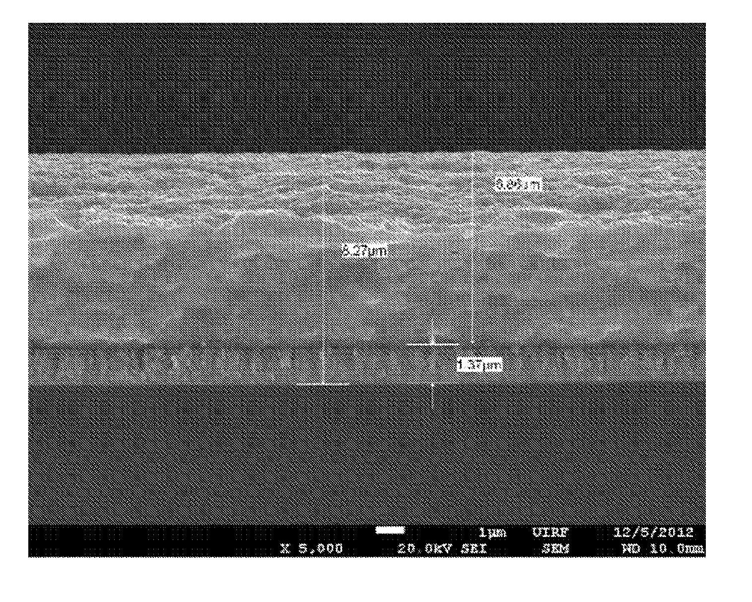
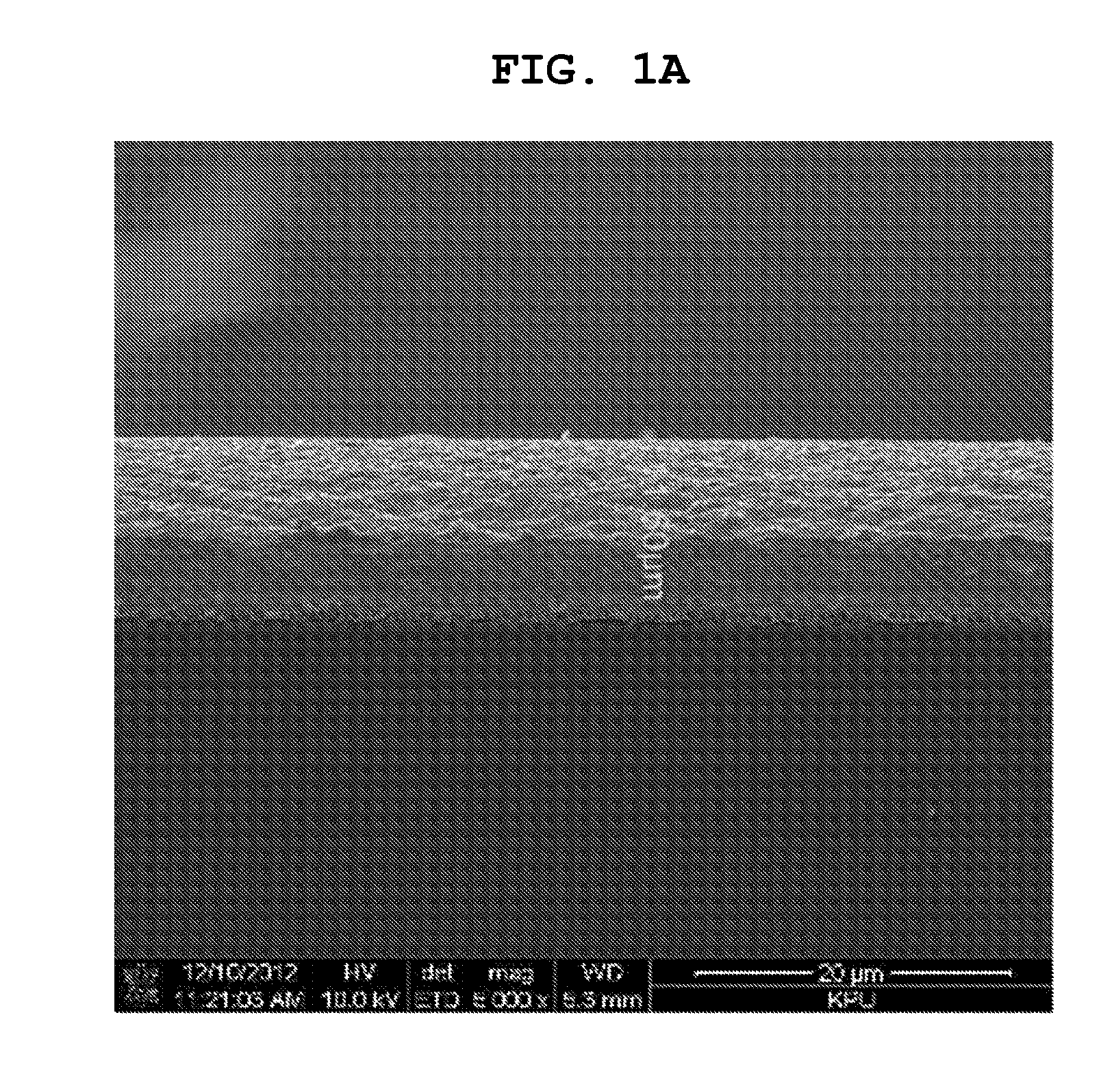
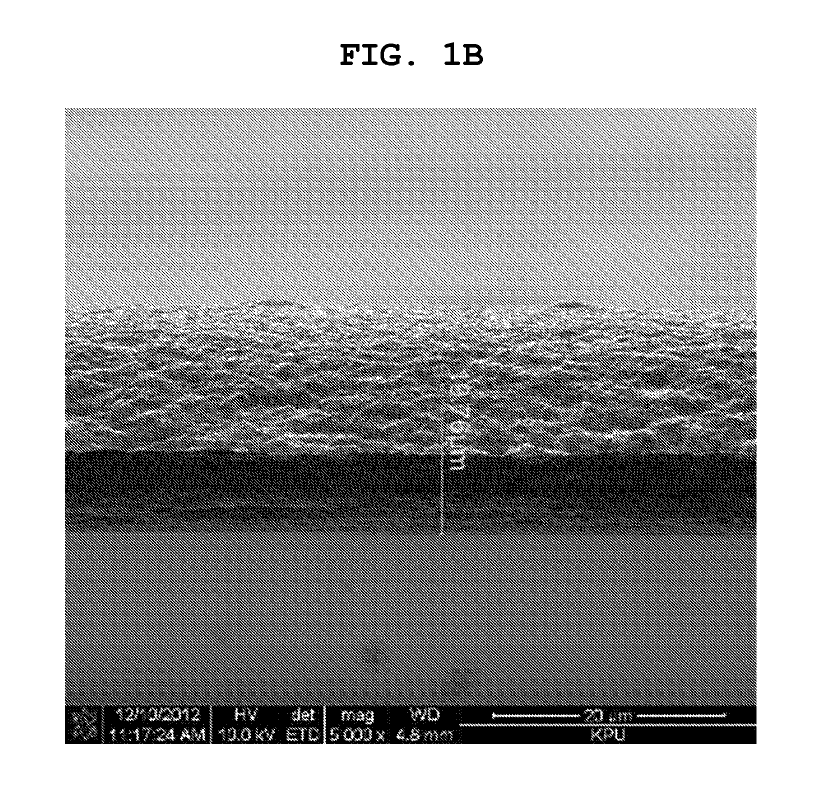
[0083]The sectional images of the iron bus bars 1 and 2 of Examples 1 and 2 and the comparative bus bars 1, 2 and 3 of Comparative Examples 1 to 3, which were observed by scanning electron microscope (SEM) to measure the total thickness of their respective coating layers, are shown in FIGS. 1A to 1E, respectively.
[0084]From FIG. 1A, it can be seen that the iron bus bar 1 includes a copper coating layer having a thickness of 11.6 μm. FIG. 1B shows that the iron bus bar 2 includes a copper coating layer having a thickness of 19.7 μm. Further, From FIGS. 1C to 1E, it can be seen that the comparative bus bars 1, 2 and 3 include coating layers having thicknesses of 3.53 μm, 3.86 μm and 8.27 μm, respectively.
PUM
| Property | Measurement | Unit |
|---|---|---|
| thickness | aaaaa | aaaaa |
| thickness | aaaaa | aaaaa |
| temperature | aaaaa | aaaaa |
Abstract
Description
Claims
Application Information


