Method for manufacturing silicon single crystal wafer and electronic device

a technology of silicon single crystal wafers and electronic devices, applied in the direction of semiconductor devices, electrical equipment, basic electric elements, etc., can solve the problems of diffusion current as a dark current increase, adverse effect, and inability to ignore, so as to achieve the effect of not affecting the device forming region

Active Publication Date: 2015-01-01
SHIN-ETSU HANDOTAI CO LTD
View PDF4 Cites 4 Cited by
  • Summary
  • Abstract
  • Description
  • Claims
  • Application Information

AI Technical Summary

Benefits of technology

[0025]Among others, the striation of oxygen that forms precipitates and has a high diffusion constant is particularly arguable. When there is the striation of oxygen, since a BMD that is formed by a BMD forming heat treatment is formed by using the oxygen striation as a template, it appears as shades of the BMD in a wafer. The formed BMD is effective as a gettering source that removes the metal contamination from a surface layer but, on the other hand, it has an adverse effect that a diffusion current as a dark current is increased since a defect level is formed. When an epitaxial layer has a large thickness, since a distance between the BMD and a device forming region is large, the diffusion current is not a serious problem, but this effect cannot be ignored and becomes obvious as a problem when a thickness of the epitaxial layer is reduced. Since this problem is greatly improved when a thickness of the epitaxial layer is increased by approximately 1 μm, the BMD that adversely affects characteristics of the solid-state image pickup device is considered to be a BMD that is produced at a position that is closest to the device forming region, i.e., a position immediately below the DZ layer.
[0053]As described above, according to the present invention, the uniform oxygen concentration peak region having high concentration can be formed near the surface of the silicon single crystal wafer. Therefore, the excellent gettering layer close to the device forming region is formed, and the device forming region is not adversely affected.

Problems solved by technology

With such a reduction in film thickness of the epitaxial layer, the following new problems have emerged.
The formed BMD is effective as a gettering source that removes the metal contamination from a surface layer but, on the other hand, it has an adverse effect that a diffusion current as a dark current is increased since a defect level is formed.
When an epitaxial layer has a large thickness, since a distance between the BMD and a device forming region is large, the diffusion current is not a serious problem, but this effect cannot be ignored and becomes obvious as a problem when a thickness of the epitaxial layer is reduced.
As a result, when the thickness of the epitaxial layer is reduced, its influence becomes obvious, and stripe image noise using the striation as the template appears in a solid-state image pickup device, thereby greatly degrading quality.
Furthermore, in a memory device, an adverse effect, e.g., an increase in leak current or a change in threshold voltage of an MOS (Metal Oxide Semiconductor) transistor is brought.

Method used


Image

  • Method for manufacturing silicon single crystal wafer and electronic device
  • Method for manufacturing silicon single crystal wafer and electronic device
  • Method for manufacturing silicon single crystal wafer and electronic device

Examples


examples 4 and 5

, Comparative Examples 4 to 6

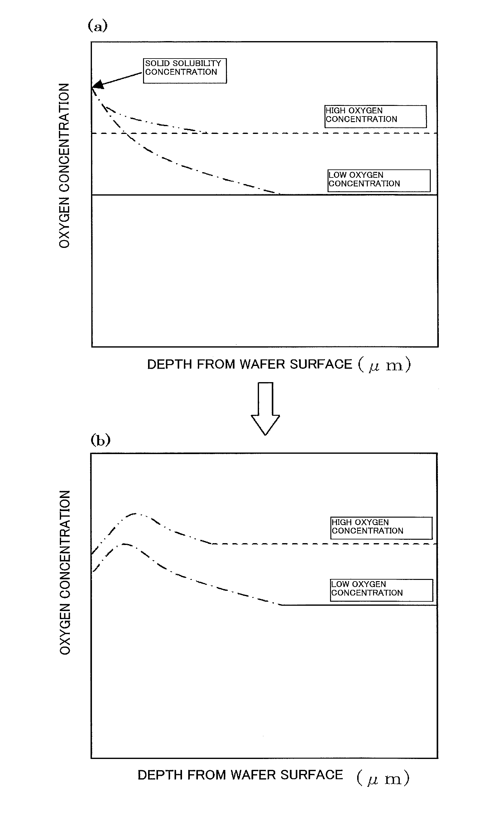
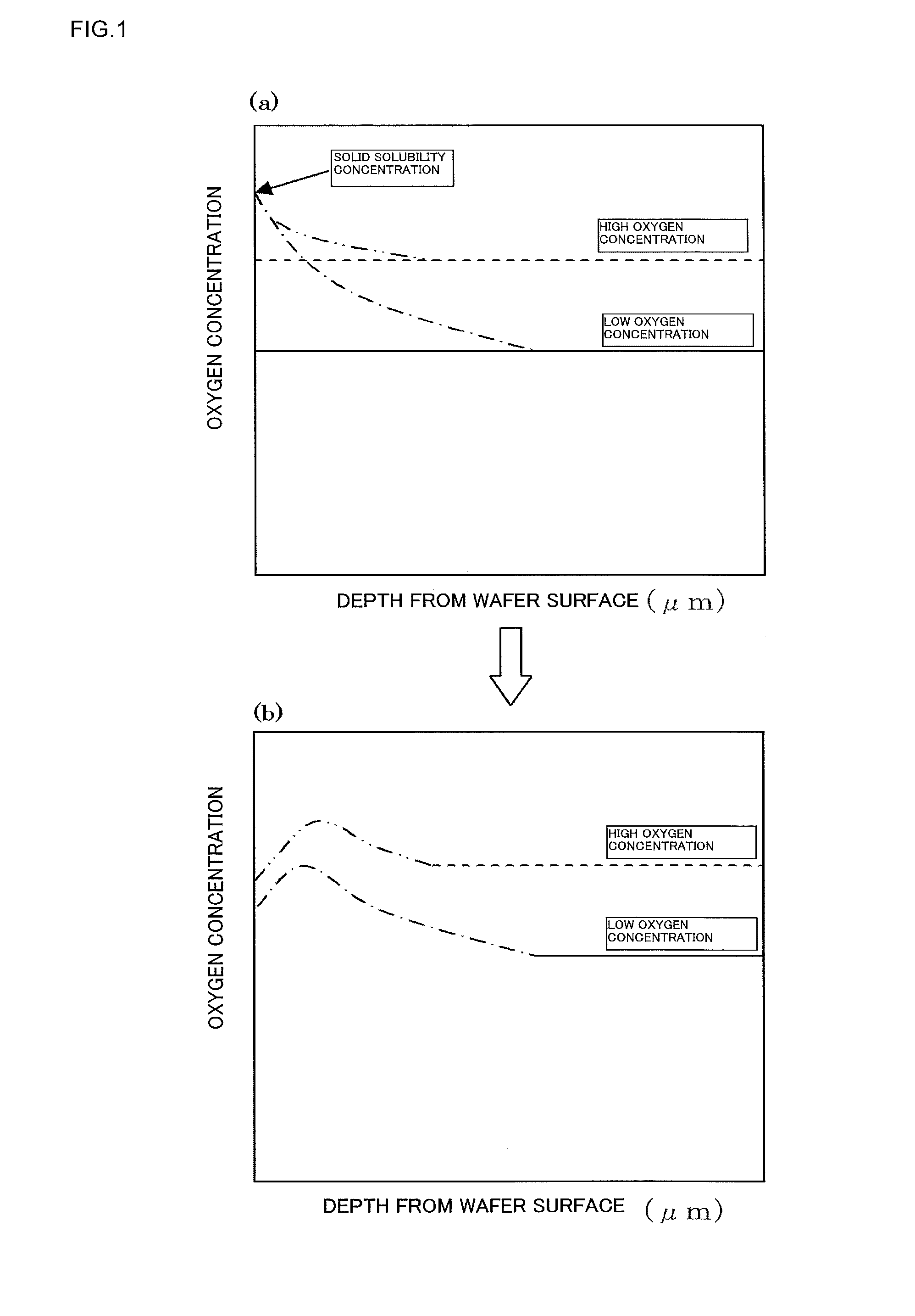
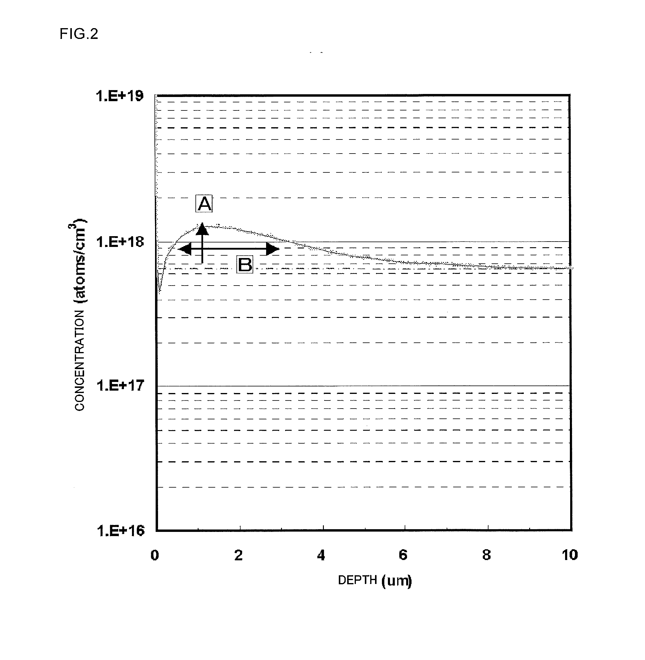
[0160]A p-type silicon single crystal ingot having oxygen concentration of 6.5×10¹⁷ atoms / cm3 and resistivity of 20 Ωcm was grown by the CZ method and sliced into a wafer shape, subjected to chamfering, lapping, and etching, then etched wafer was subjected to double-side polishing on both front and back sides thereof, and one main surface of double-side polished wafer was subjected to final mirror polishing. As a result, each double-side polished wafer (a DSP wafer) having a diameter of 12 inches (300 mm) and a thickness of 775 μm was prepared.

[0161]Subsequently, a commercially available RTA apparatus (Helios manufactured by Mattson) was used to perform a rapid heating / rapid cooling heat treatment (the RTA treatment), i.e., an oxygen inward diffusion heat treatment for increasing a temperature from a room temperature to 1350° C. in a 100% oxygen atmosphere at a temperature increasing rate of 50° C. / second, holding each wafer for 10 seconds, and then lowe...


PUM

PropertyMeasurementUnit
temperatureaaaaaaaaaa

Abstract

According to the present invention, there is provided a method for manufacturing a silicon single crystal wafer, wherein a first heat treatment for holding a silicon single crystal wafer in an oxygen containing atmosphere at a first heat treatment temperature for 1 to 60 seconds and cooling it to 800° C. or less at a temperature falling rate of 1 to 100° C. / second by using a rapid heating / rapid cooling apparatus is performed to inwardly diffuse oxygen and form an oxygen concentration peak region near a surface of the silicon single crystal wafer, and then a second heat treatment is performed to agglomerate oxygen in the silicon single crystal wafer into the oxygen concentration peak region. As a result, it is possible to provide the method for manufacturing a silicon single crystal wafer that enables forming an excellent gettering layer close to a device forming region.

Description

BACKGROUND OF THE INVENTION[0001]1. Field of the Invention[0002]The present invention relates to a method for manufacturing a silicon single crystal wafer that is suitable for fabrication of an image pickup device or a memory device and to an electronic device using this method.[0003]2. Description of the Related Art[0004]A silicon single crystal wafer for use in a semiconductor device is generally sliced out from a silicon single crystal ingot grown by a Czochralski method (which will be referred to as a [CZ method] hereinafter) and manufactured through processes such as polishing. Request items required for this silicon single crystal wafer are formation of a defect-free layer (a Denuded Zone layer: which will be referred to as a [DZ layer] hereinafter) in a surface layer, control over solid solubility oxygen concentration that affects mechanical strength, and control over an oxide precipitate (a Bulk Micro Defect: which will be referred to as a [BMD] hereinafter) formed in the wa...

Claims


Application Information

Patent Timeline
Patent Type & Authority Applications(United States)
IPC IPC(8): H01L21/322H01L29/16
CPCH01L29/16H01L21/3225
Inventor OKA, TETSUYAEBARA, KOJI
Owner SHIN-ETSU HANDOTAI CO LTD
Why Eureka
Try Eureka