Electrostatic capacitance transducer, probe, and subject information acquiring device

a technology of electrically charged capacitance and transducer, which is applied in the direction of mechanical vibration separation, instruments, and using reradiation, can solve the problems of poor transmission/reception properties and parasitic capacitance between lines, and achieve the effect of suppressing parasitic capacitance and reducing parasitic capacitan

Active Publication Date: 2015-01-15
CANON KK
View PDF7 Cites 12 Cited by
  • Summary
  • Abstract
  • Description
  • Claims
  • Application Information

AI Technical Summary

Benefits of technology

[0009]However, simply connecting multiple elements and multiple lines on the flexible printed circuit at the edges of element substrates results in narrow intervals between adjacent lines, which can cause parasitic capacitance between the lines. This can then result in poorer transmission / reception properties (conversion efficiency).
[0010]It has been found desirable to provide an electrostatic capacitance transduce with suppressed deterioration in conversion efficiency, by reducing parasitic capacitance between lines.

Problems solved by technology

However, simply connecting multiple elements and multiple lines on the flexible printed circuit at the edges of element substrates results in narrow intervals between adjacent lines, which can cause parasitic capacitance between the lines.
This can then result in poorer transmission / reception properties (conversion efficiency).

Method used


Image

  • Electrostatic capacitance transducer, probe, and subject information acquiring device
  • Electrostatic capacitance transducer, probe, and subject information acquiring device
  • Electrostatic capacitance transducer, probe, and subject information acquiring device

Examples


first embodiment

Configuration of Electrostatic Capacitance Transducer

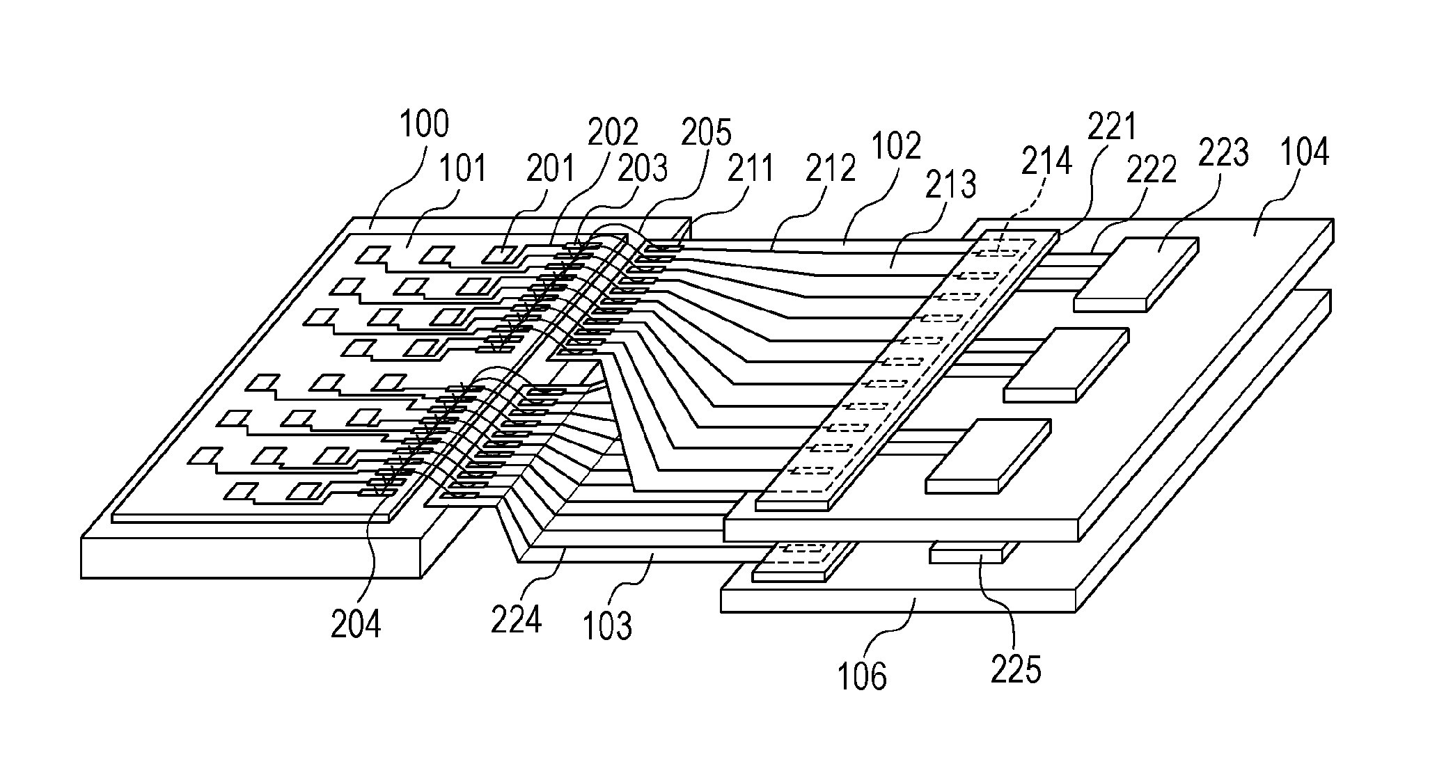
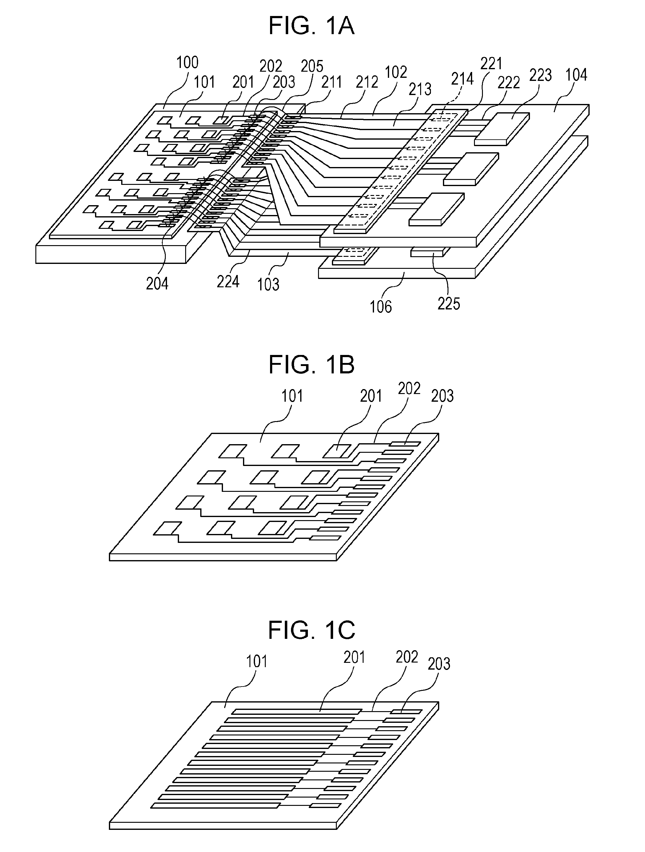
[0026]The overall configuration of an electrostatic capacitance transducer according to a first embodiment will be described with reference to FIGS. 1A through 1C. FIG. 1A is a perspective view of the electrostatic capacitance transducer, and FIGS. 1B and 1C are perspective views of an element chip. The electrostatic capacitance transducer according to the present embodiment is capable of at least one of transmission and reception of acoustic waves (typically ultrasound).

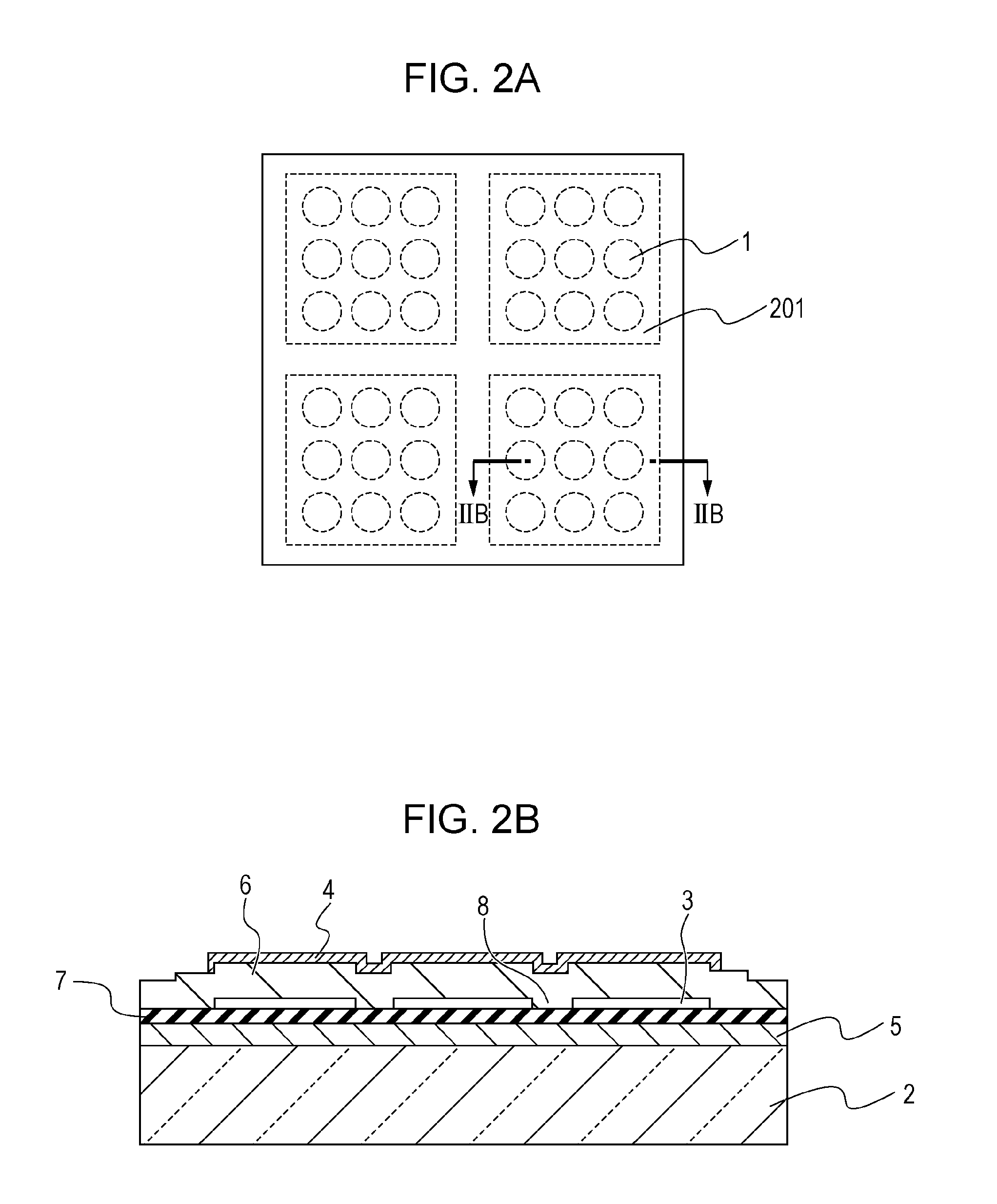
[0027]The electrostatic capacitance transducer according to the present embodiment includes an element chip 101, a first flexible printed circuit 102, and a second flexible printed circuit 103. The element chip 101 includes multiple elements 201 provided upon a substrate 2. The multiple elements 201 may be arranged in a two-dimensional array such as illustrated in FIG. 1B, or in a one-dimensional array such as illustrated in FIG. 1C. The multiple elements 201 incl...

second embodiment

[0057]A second embodiment will be described with reference to FIG. 5. This embodiment relates to the configuration of electrical connection between the element chip and flexible printed circuits. Other configurations are the same as with the first embodiment, and according description will be omitted.

[0058]A feature of the present embodiment is that the element chip 101, and the first and second flexible printed circuits 102 and 103, are electrically connected using an anisotropic conductive film (ACF). FIG. 5A is a schematic diagram of an electrostatic capacitance transducer according to the present embodiment, and FIGS. 5B and 5C are plan views of the element chip 101.

[0059]In the present embodiment, the element chip 101, and the first and second flexible printed circuits 102 and 103, are connected at an end of the element chip 101. The first and second electrode pads 203 and 204 arrayed at the end of the element chip 101 are electrically connected to wiring pads 211 on the first ...

third embodiment

[0068]A third embodiment will be described with reference to FIG. 6. This embodiment relates to wiring on multiple flexible printed circuits. Other configurations are the same as in the first and second embodiments, so description thereof will be omitted.

[0069]A feature of this embodiment is that first wires 241 of the first flexible printed circuit 102 and second wires 242 of the second flexible printed circuit 103 are in offset regions when viewed in the thickness direction of the first and second flexible printed circuits. FIG. 6 is a transparent view of multiple flexible printed circuits from above the flexible printed circuits.

[0070]In FIG. 6, the first flexible printed circuit 102 and the second flexible printed circuit 103 are overlaid at a region on the circuit substrate side. Within this region on the circuit substrate side, the second wires 242 on the second flexible printed circuit 103 are offset as to the first wires 241 on the first flexible printed circuit 102 by aroun...


PUM


Abstract

An electrostatic capacitance transducer includes: multiple elements each having a cell including a first electrode, and a vibrating film including a second electrode, formed across a gap from the first electrode; a first flexible printed circuit having multiple first lines; and a second flexible printed circuit having multiple second lines. Part of the multiple elements are grouped into a first element group, each one thereof being electrically connected to a different one of the first lines. Part of the multiple elements other than the first element group are grouped into a second element group, each one thereof being electrically connected to a different one of the second lines. The intervals between adjacent lines in at least part of the plurality of first and second lines are wider at an opposite side from a connection side where the lines have been connected to the multiple elements, than at the connection side.

Description

BACKGROUND OF THE INVENTION[0001]1. Field of the Invention[0002]The present invention relates to an electrostatic capacitance transducer, a probe, and a subject information acquiring device, and more particularly relates to an electrostatic capacitance transducer relating to a technology in which at least one of transmission and reception of acoustic waves, and to a probe and subject information acquiring device including the same.[0003]2. Description of the Related Art[0004]Capacitive micromachined ultrasonic transducers (CMUT), which are a type of electrostatic capacitance transducer, are being studies as a substitute for piezoelectric elements. CMUTs are manufactured using a microelectromechanical systems (MEMS) process employing a semiconductor processing, as described in “Capacitive micromachined ultrasonic transducers: fabrication technology,” Ultrasonics, Ferroelectrics and Frequency Control, IEEE Transactions on, vol. 52, no. 12, pp. 2242-2258, December 2005.[0005]A CMUT cel...

Claims


Application Information

Patent Timeline
Patent Type & Authority Applications(United States)
IPC IPC(8): G10K9/12G01S15/02H02N1/00
CPCH02N1/006G10K9/12G01S15/02B06B1/0292H05K1/0228H05K1/0243H05K1/025H05K1/147H05K2201/09227H05K2201/10189H04R19/00
Inventor KANDORI, ATSUSHI
Owner CANON KK
Why Eureka
Try Eureka