Light-emitting diode and method of manufacturing the same

a technology of light-emitting diodes and manufacturing methods, which is applied in the field of light-emitting diodes and, can solve the problems of difficult formation of protective films, electrical conduction failures, and film or electrode metal films are likely to be discontinuous films, and achieve high light emission output, improve light extraction efficiency, and high efficiency

Active Publication Date: 2015-02-05
SHOWA DENKO KK
View PDF3 Cites 24 Cited by
  • Summary
  • Abstract
  • Description
  • Claims
  • Application Information

AI Technical Summary

Benefits of technology

[0027]A light-emitting diode according to an aspect of the invention includes a reflecting layer that consists of metal and a compound semiconductor layer sequentially including an active layer and a contact layer which are sequentially provided on a supporting substrate, and outputs light from a light emission hole to the outside. In addition, the light-emitting diode includes a transparent conductive film that is provided between the reflecting layer and the compound semiconductor layer at a position that corresponds to the electrical conduction window and in a range surrounded by the electrical conduction window in plane view. As a result, the amount of light emitted from a portion of the active layer which is arranged immediately below the electrical conduction window and the range surrounded by the electrical conduction window is more than the amount of light emitted from a portion other than the portion which is arranged immediately below the electrical conduction window and the range. In addition, the reflecting layer reflects light which travels from a light-emitting layer to the supporting substrate with high efficiency. Therefore, the percentage of light which travels toward the light emission hole increases and light extraction efficiency is improved.
[0028]The light-emitting diode according to the aspect of the invention includes the flat portion and the mesa structure portion including the inclined side surface and the top surface that are provided in its upper part. As a result, it is possible to obtain a high light emission output and to input the emitted light to, for example, an optical component with high efficiency.
[0029]In the light-emitting diode according to the aspect of the invention, the inclined side surface of the mesa structure portion is formed by wet etching such that the cross-sectional area thereof in the horizontal direction is continuously reduced toward the top surface. As a result, it is easy to sequentially form the protective film and the electrode film on the side surface of the mesa structure portion, as compared to a case in which the mesa structure portion has a vertical side surface. Therefore, a continuous film with a uniform thickness is formed. As a result, leakage or electrical conduction failure caused by a discontinuous film does not occur and stable and high-brightness light emission is ensured. This effect is obtained when the light-emitting diode has the mesa structure portion with the inclined side surface which is formed by wet etching, regardless of the internal laminated structure of the light-emitting diode or the structure of the substrate.
[0030]In the light-emitting diode according to the aspect of the invention, the transparent conductive film is made of any one of ITO, IZO, and ZnO. Therefore, the operating voltage is reduced by high conductivity and high transmittance of light reflected from the reflecting layer is ensured. As a result, a high output is obtained.
[0031]The light-emitting diode according to the aspect of the invention includes an ohmic metal portion that consists of AuBe or AuZn and is provided in a peripheral portion of the transparent conductive film which does not overlap the light emission hole in plane view, between the transparent conductive film and the compound semiconductor layer. Therefore, a sufficient ohmic contact with the contact layer is ensured and a transparent portion which is covered with the ohmic metal portion is formed in the transparent conductive film at a position immediately below the light emission hole. As a result, most light which is reflected by the reflecting layer and passes through the transparent portion is emitted from the light emission hole.
[0032]In the light-emitting diode according to the aspect of the invention, the contact layer comes into contact with the electrode film. According to this structure, the contact resistance of an ohmic electrode is reduced and low-voltage driving can be performed.

Problems solved by technology

However, it is not easy to form the protective film or the electrode metal film on the vertical side surface or the steeply inclined side surface with a uniform thickness and the protective film or the electrode metal film is likely to be a discontinuous film.
In addition, when the electrode metal film is a discontinuous film (letter B in FIG. 16), an electrical conduction failure occurs.
When the portion other than the pillar structure is removed by dry etching, an expensive apparatus is required and the etching time increases.
Therefore, light extraction efficiency is not improved.

Method used


Image

  • Light-emitting diode and method of manufacturing the same
  • Light-emitting diode and method of manufacturing the same
  • Light-emitting diode and method of manufacturing the same

Examples


first embodiment

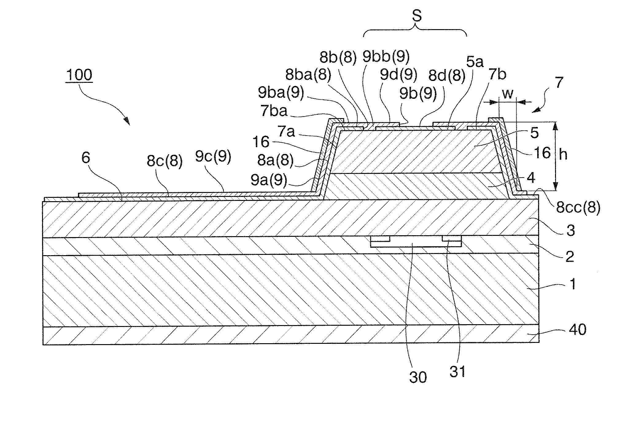
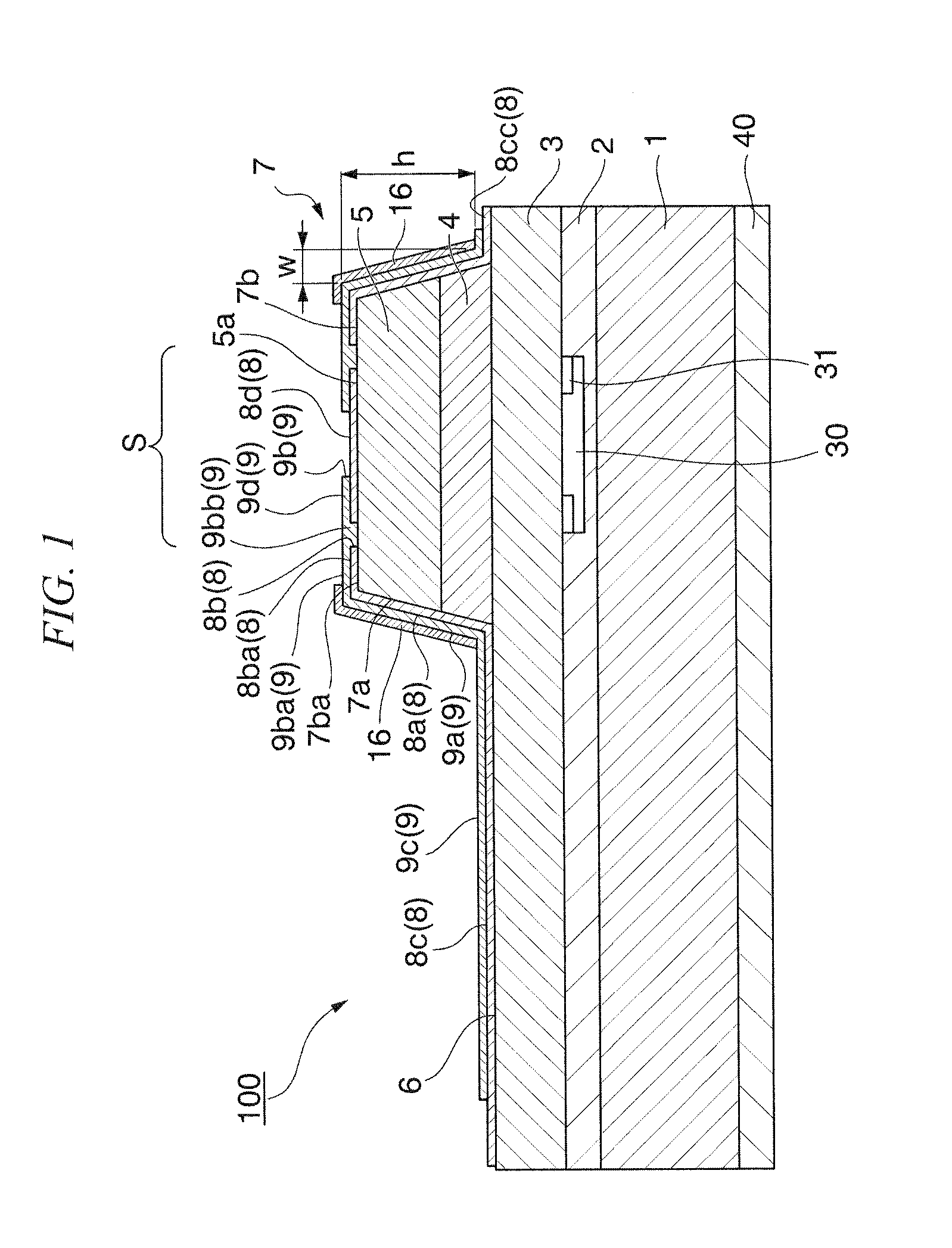
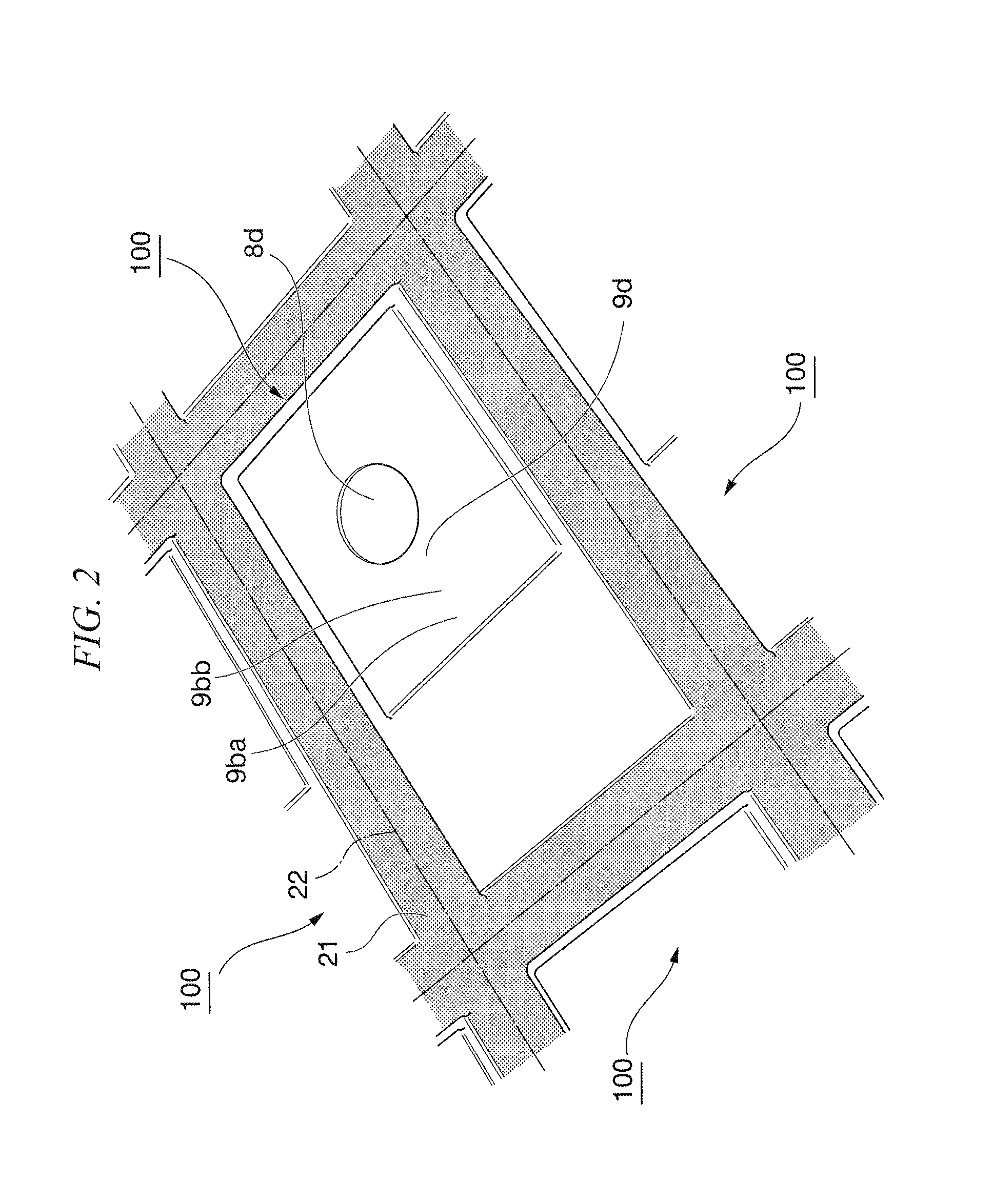
[0063]FIG. 1 is a schematic cross-sectional view illustrating an example of a light-emitting diode to which the invention is applied. FIG. 2 is a perspective view illustrating the light-emitting diode formed on a wafer including the light-emitting diode shown in FIG. 1.

[0064]Hereinafter, a light-emitting diode according to an embodiment of the invention will be described in detail with reference to FIGS. 1 and 2.

[0065]A light-emitting diode 100 shown in FIG. 1 includes a reflecting layer 2 which consists of metal and a compound semiconductor layer 20 (see FIG. 4) that includes an active layer 4 and a contact layer 5 in this order, which are sequentially provided on a supporting substrate 1, and emits light from a light emission hole 9b to the outside. The light-emitting diode includes a flat portion 6 and a mesa structure portion 7 including an inclined side surface 7a and a top surface 7b in its upper part. The flat portion 6 and the mesa structure portion 7 are at least partially ...

second embodiment

[0161]FIG. 6 is a schematic cross-sectional view illustrating another example of the light-emitting diode which is an example of the light-emitting diode to which the invention is applied.

[0162]In the first embodiment, the protective film is formed below the light emission hole and light is extracted from the light emission hole through the protective film in the top surface of the mesa structure portion. A second embodiment has a structure in which the protective film is not provided below the light emission hole and light is directly extracted from a light emission hole 9b, without passing through the protective film.

[0163]That is, in a light-emitting diode 200 according to the second embodiment, a protective film 28 covers at least a portion 28c of a flat portion 6, an inclined side surface 7a of a mesa structure portion 7, and a peripheral region 7ba of a top surface 7b of the mesa structure portion 7. In addition, the protective film 28 includes an electrical conduction window ...

modification example

[0169]FIGS. 7(a) to 7(c) are schematic cross-sectional views illustrating a portion of the metal substrate for describing a process of manufacturing the metal substrate.

[0170]A first metal layer (first metal plate) 51b which has a larger thermal expansion coefficient than the material forming the active layer and a second metal layer (second metal plate) 51a which has a smaller thermal expansion coefficient than the material forming the active layer are used as the metal substrate 1 and the substrate 1 is formed by performing a hot press.

[0171]Specifically, first, two first metal layers 51b which are substantially flat plates and one second metal layer 51a which is a substantially flat plate are prepared. For example, a Cu layer with a thickness of 10 μm is used as the first metal layer 51b and a Mo layer with a thickness of 75 μm is used as the second metal layer 51a.

[0172]Then, as shown in FIG. 7(a), the second metal layer 51a is inserted between the two first metal layers 51b so...


PUM


Abstract

A light-emitting diode and manufacturing method, including a flat portion and a mesa structure. An inclined side surface is formed by wet etching such that a cross-sectional area of the mesa structure is continuously reduced toward a top surface. A protective film covers the flat portion, the inclined side surface, and a peripheral region of the top surface of the mesa structure. The protective film includes an electrical conduction window arranged around a light emission hole and from which a compound semiconductor layer is exposed. A continuous electrode film contacts the exposed compound semiconductor layer, covers the protective film formed on the flat portion, and has the light emission hole on the top surface. A transparent conductive film is formed between a reflecting layer and the layer at a position that corresponds to the electrical conduction window and in a range surrounded by the electrical conduction window.

Description

FIELD OF THE INVENTION[0001]The present invention relates to a light-emitting diode and a method of manufacturing the same.[0002]Priority is claimed on Japanese Patent Application No. 2011-277535, filed on Dec. 19, 2011, the content of which is incorporated herein by reference.DESCRIPTION OF RELATED ART[0003]A point light source type light-emitting diode is known in which light generated by a light-emitting layer is extracted from a portion of the upper surface of an element. In this type of light-emitting diode, a light-emitting diode is known which has a current-blocking structure for limiting an electrically conductive region of a light-emitting layer to a portion of the plane of the light-emitting layer (for example, see Patent Document 1). In the light-emitting diode having the current-blocking structure, a light-emitting region is limited. Since light is emitted from a light emission hole which is provided immediately above this light-emitting region, it is possible to obtain ...

Claims


Application Information

Patent Timeline
Patent Type & Authority Applications(United States)
IPC IPC(8): H01L33/24H01L33/00H01L33/44H01L33/30H01L33/42H01L33/06H01L33/10
CPCH01L33/24H01L33/06H01L33/005H01L33/10H01L2933/0058H01L33/42H01L33/44H01L2933/0016H01L2933/0025H01L33/30H01L33/20H01L33/38H01L33/405H01L33/385H01L33/0062H01L33/0093
Inventor AIHARA, NORIYUKI
Owner SHOWA DENKO KK
Why Eureka
Try Eureka