Process for making materials with micro- or nanostructured conductive layers

a technology of conductive layers and materials, applied in the direction of sustainable manufacturing/processing, mechanical vibration separation, final product manufacturing, etc., can solve the problems of low processing cost, complex and time-consuming modifications, and need for a bendable replacement with low processing cost, and achieve cost-efficient and scalable effects

Inactive Publication Date: 2015-02-05
SABIC GLOBAL TECH BV
View PDF6 Cites 54 Cited by
  • Summary
  • Abstract
  • Description
  • Claims
  • Application Information

AI Technical Summary

Benefits of technology

[0007]A solution to avoiding the use of the aforementioned pre-conditioning steps has been discovered. The discovery is based on the simultaneous application of both heat and pressure to micro-structures or nanostructures (or a combination of both micro- and nanostructures) that have been deposited onto a substrate, the result of which is ...

Problems solved by technology

The inorganic semiconductor, indium tin oxide (ITO), is the most widely used material as the transparent conducting electrode, but the lack of flexibility and rising price due to limited earth abundance underscore the need for a bendable replacement with lo...

Method used


Image

  • Process for making materials with micro- or nanostructured conductive layers
  • Process for making materials with micro- or nanostructured conductive layers
  • Process for making materials with micro- or nanostructured conductive layers

Examples


example 1

Materials and Methods for Transparent / Translucent Electrodes

[0068]Materials.

[0069]100 micron-thick PET film substrates were provided by SABIC; the Tg of the PET film was reported to be 75° C. Lithium fluoride (LiF), silver chloride (AgCl), potassium bromide (KBr), silver nitrate (AgNO3), polyvinylpyrrolidone (PVP) and ethylene glycol were purchased from Sigma Aldrich and used without any further purification. Solvents were purchased from available commercial sources and used as received unless mentioned otherwise. Aluminum was received in pellets from Kurt J. Lesker. For the active layer of the OPV devices, the PC61BM and P3HT were purchased from American Dye Source and Reike Metals Inc., respectively. PEDOT:PSS (PVP AI 4083) was purchased from Heraeus. ITO was purchased from Delta Technologies and had a sheet resistance of 8-12Ω / □. Before organic photovoltaic device fabrication the ITO was cleaned with successive 10 minute sonication steps in methylene chloride, deionized water, an...

example 2

Results for Transparent / Translucent Electrodes

[0080]Produced Conductive Materials:

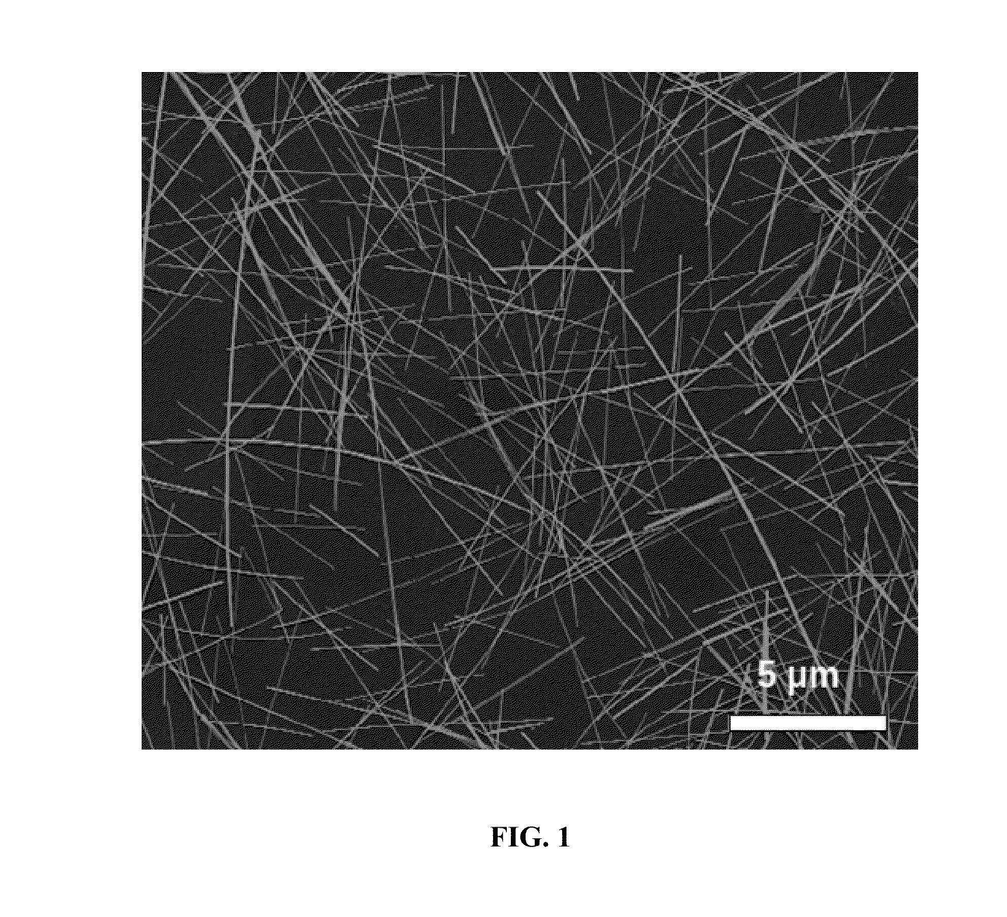
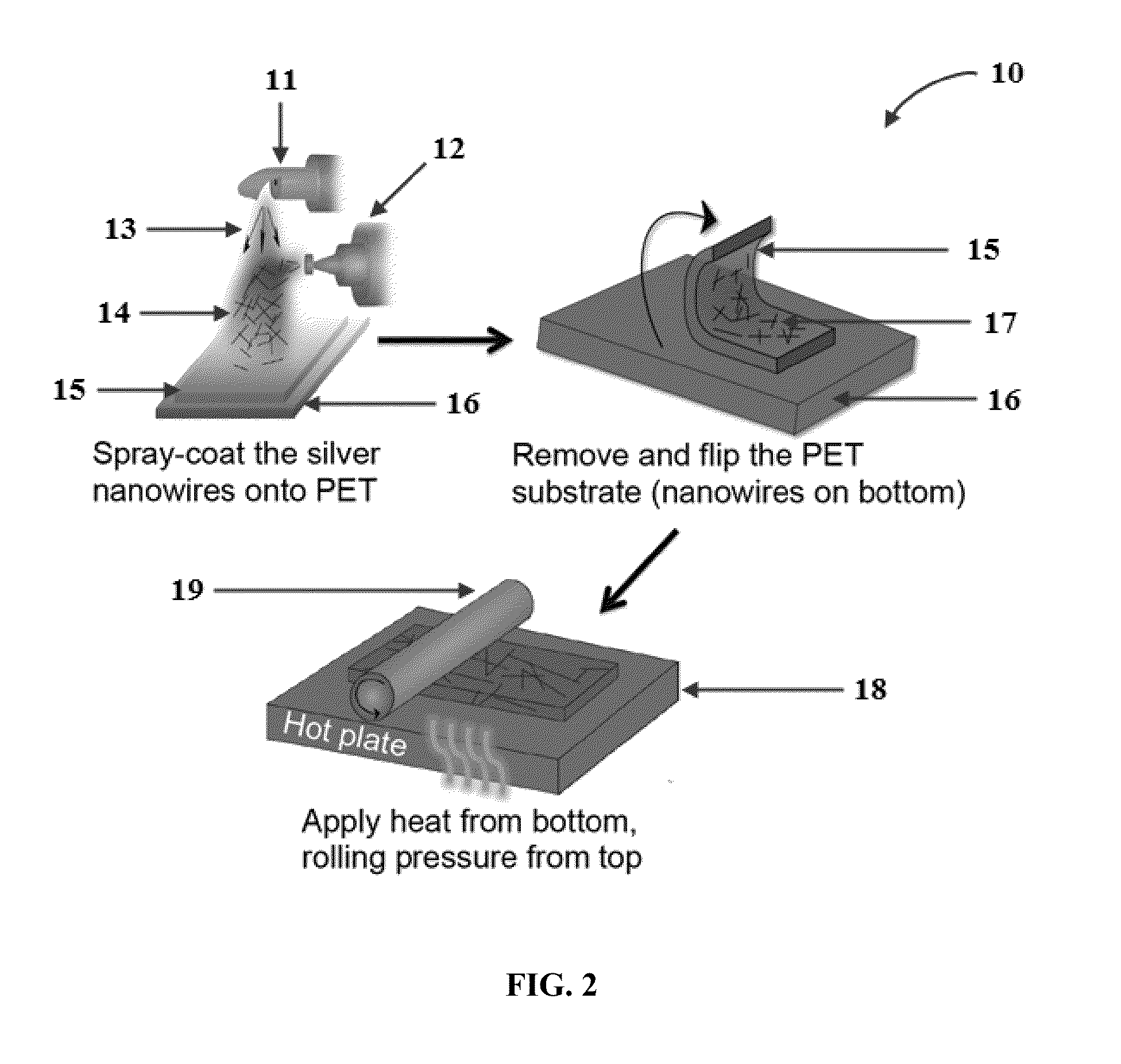
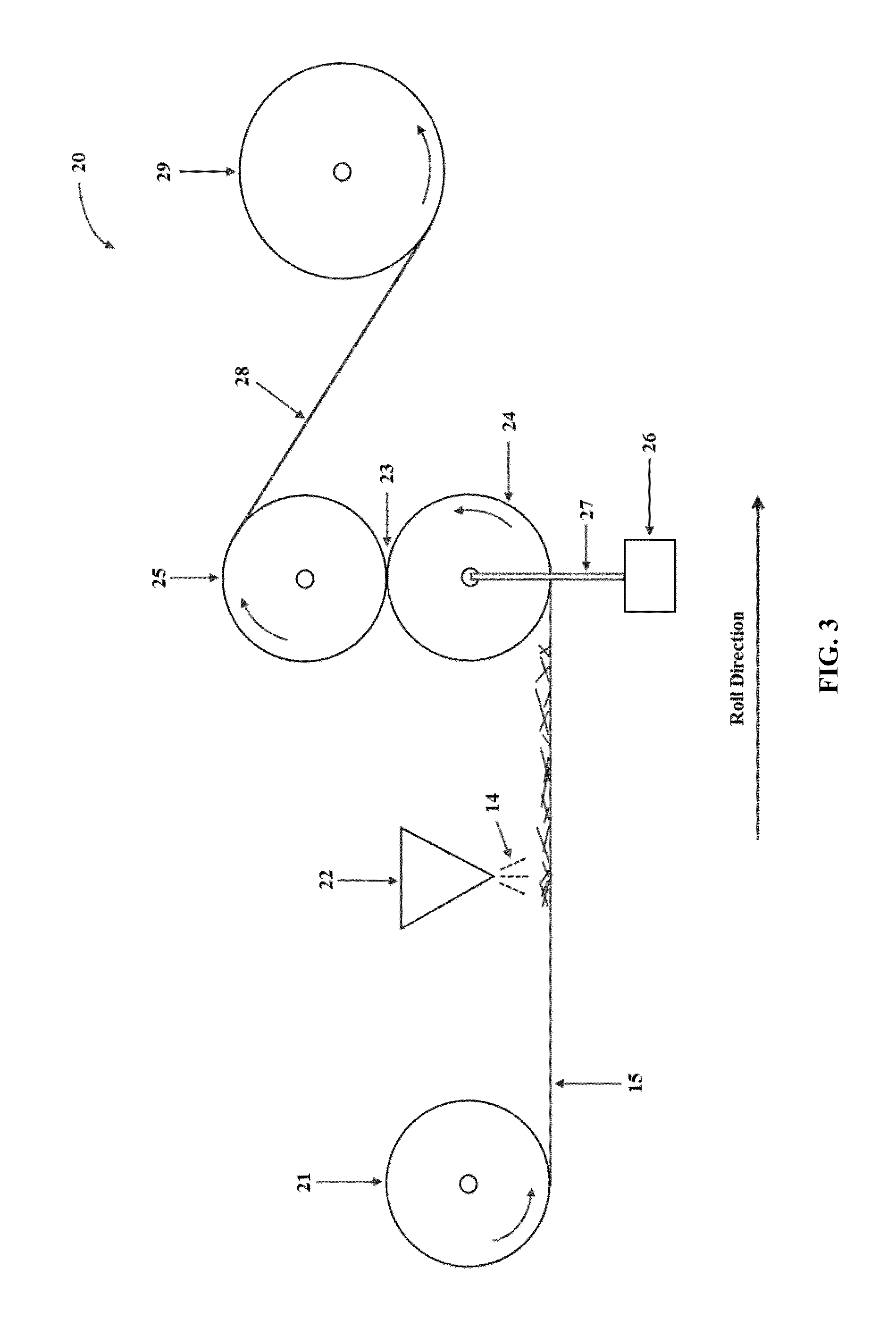
[0081]Silver nanowires with diameters of 50-100 nm, and lengths of 5-10 microns were prepared via a straightforward solution phase procedure (Hu, et al., 2010). A representative example of a spray-coated silver nanowire mesh on PET is shown in the scanning electron microscope (SEM) image in FIG. 1. The commercial PET films from SABIC were 100 microns thick, with a reported Tg of 75° C. and a Vicat softening temperature of 79° C. and 75° C. for the Vicat A and Vicat B tests respectively. FIG. 2 provides the schematic outline of the electrode processing described: the silver nanowires were spray-coated onto cleaned PET, removed from the spray-coater, and turned over onto a polished stainless steel hot plate with the nanowires in contact with the hot plate surface at the desired temperature. The back of the PET film was then rolled with a stainless steel rod (radius=30 mm), and then removed and allowed to...

example 3

Reflective Electrode Data

[0097]Reflective electrodes using a transparent substrate (PET) were prepared in the same manner discussed above in Example 1 with one difference. Additional nanowires were used to increase the reflectivity of the resulting electrode. FIGS. 12A and 12B provide normal and total reflection data, respectively. The plots in FIGS. 12A and 12B show a comparison between optically thick electrodes that are as deposited, meaning sprayed on the PET and left as is, and processed, meaning sprayed followed by rolling with pressure / heat. The dashed line represents the as-deposited sample while the solid is the processed sample. There is an increase in both the normal reflection and total reflection. Normal reflection refers to specular reflection where in incident angle is equal to the output angle. In this case the angle of incidence was small (˜8°) which can be approximated to normal. The total reflection was measured using an integrating sphere and compared against cer...


PUM

PropertyMeasurementUnit
Fractionaaaaaaaaaa
Fractionaaaaaaaaaa
Fractionaaaaaaaaaa

Abstract

Disclosed are methods for making conductive materials. The methods can be used to make transparent, opaque, or reflective electrodes by using the same materials and equipment but varying the processing conditions or amounts of materials used. The methods can include: (a) providing a substrate comprising a first surface and an opposite second surface, wherein micro- or nanostructures are disposed on at least a portion of the first surface, and wherein the first surface is not pre-conditioned to increase attachment between the micro- or nanostructures and the substrate; (b) applying heat to heat the substrate surface to a temperature that is greater than the glass transition temperature or the Vicat softening temperature of the substrate and less than the melting point of the substrate; (c) applying pressure such that the substrate and the micro- or nanostructures are pressed together; and (d) removing the pressure to obtain the conductive material.

Description

CROSS-REFERENCE TO RELATED APPLICATIONS[0001]This application claims the benefit of U.S. Provisional Application No. 61 / 860,485, filed Jul. 31, 2013, the contents of which are incorporated by reference.BACKGROUND OF THE INVENTION[0002]A. Field of the Invention[0003]The invention generally concerns a process for making electrically conductive materials that can be used in a wide-array of applications and electronic devices. In particular, the invention concerns a process for making a conductive micro- or nanostructured layer on at least a portion of the surface of a substrate by simultaneous application of heat and pressure to sufficiently attach disposed micro- or nanostructures to the substrate's surface and to create the conductive micro or nanostructured layer from the disposed micro- or nanostructures. Notably, no pre-conditioning steps of the substrate's surface are needed to sufficiently attach the conductive structures to the substrate.[0004]B. Description of Related Art[0005...

Claims


Application Information

Patent Timeline
IPC IPC(8): H01B13/00B05D1/18B05D1/32B05D3/02B05D1/28B05D1/26B05D3/12B05D1/02B05D1/00
CPCH01B13/0016H01B13/0026B05D1/02B05D1/18B05D3/0254B05D1/005B05D1/28B05D1/26B05D3/12B05D1/32Y02E10/549Y02P70/50H10K71/60H10K85/1135H10K85/113H10K30/30
Inventor BURIAK, JILLIAN M.HAUGER, TATE C.AL-RAFIA, S. M. IBRAHIMTEVTIA, AMIT K.ABDELRAHMAN, AHMED I.ODEH, IHAB
Owner SABIC GLOBAL TECH BV
Why Eureka
Try Eureka