
Single crystal copper, manufacturing method thereof and substrate comprising the same

a manufacturing method and single crystal technology, applied in the direction of crystal growth process, printing, metallic pattern materials, etc., can solve the problems of small grain contamination, failure to fully grow, and bulky single crystal copper grain, etc., to improve industrial applicability, excellent characteristics such as mechanical, electrical and light properties, heat stability and electromigration resistan

Inactive Publication Date: 2015-03-05
NAT CHIAO TUNG UNIV
View PDF5 Cites 9 Cited by
  • Summary
  • Abstract
  • Description
  • Claims
  • Application Information

AI Technical Summary

Benefits of technology

The present invention provides a method for producing high-quality single crystal copper with a specific orientation and large grain size. This copper has excellent characteristics such as strength, electrical conductivity, light properties, heat stability, and resistance to electromigration, which makes it highly useful in various industrial applications.

Problems solved by technology

However, there are two major deficiencies in the prior art.
First, the single crystal copper grain is a bulk and cannot be directly grown on a silicon substrate for use in the microelectronics industry.
Moreover, with reference to the recent related articles by Jun Liu et al., although the growth orientation of copper crystal can be controlled and a large grain can be obtained by optimizing the electroplating parameters of the pulse electroplating, the obtained crystal suffers from the problem of having contaminant of small grain copper, failing to fully grow as single crystal copper (referring to Jun Liu, Changqing Liu, Paul P Conway, “Growth mechanism of copper column by electrodeposition for electronic interconnections,” Electronics Systemintegration Technology Conference, p 679-84 (2008) and Jun Liu, Changqing Liu, Paul P Conway, Jun Zeng, Changhai Wang, “Growth and Recrystallization of Electroplated Copper Columns,” International

Method used


Image

  • Single crystal copper, manufacturing method thereof and substrate comprising the same
  • Single crystal copper, manufacturing method thereof and substrate comprising the same
  • Single crystal copper, manufacturing method thereof and substrate comprising the same

Examples


Embodiment Construction

[0039]Hereinafter, the actions and the effects of the present invention will be explained in more detail via specific examples of the invention. However, these examples are merely illustrative of the present invention and the scope of the invention should not be construed to be defined thereby.

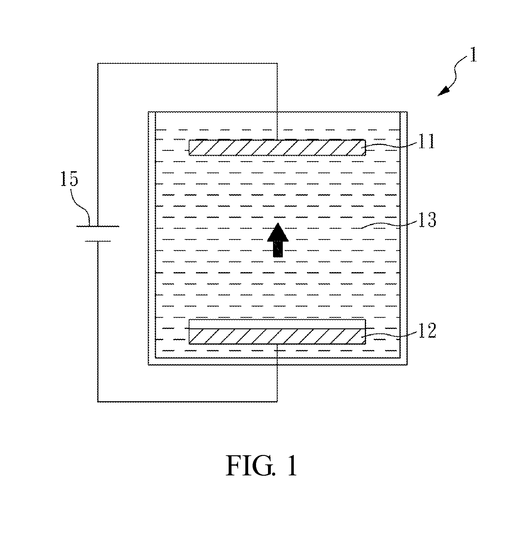
[0040]The electroplating apparatus shown in FIG. 1 is provided, which comprises: an anode 11, a cathode 12, an electroplating solution 13, and a power supply 15, wherein the power supply 15 is connected to the anode 11 and the cathode 12 respectively, and the anode 11 and the cathode 12 are dipped in the electroplating solution 13.

[0041]In this case, the anode 11 is made of a commercial 99.99% pure copper target, the cathode 12 is a silicon chip, and the electroplating solution 13 comprises copper sulfate (Cu ion concentration of 20-60 g / L), chloride ions (10-100 ppm), and methanesulfonic acid (80-120 g / L), and may be optionally added with other surfactants or lattice modifiers (such as 1-100 ...


PUM

PropertyMeasurementUnit
volumeaaaaaaaaaa
thicknessaaaaaaaaaa
thicknessaaaaaaaaaa

Abstract

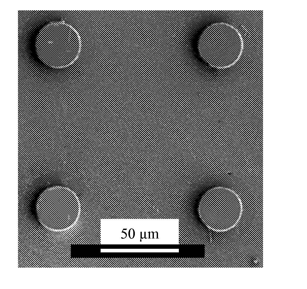
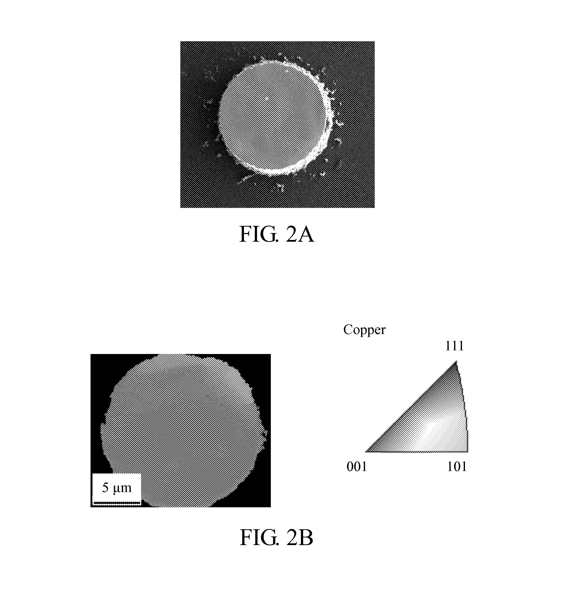
The present invention relates to a single crystal copper having [100] orientation and a volume of 0.1˜4.0×106 μm3. The present invention further provides a manufacturing method for the single crystal copper and a substrate comprising the same.

Description

CROSS REFERENCE TO RELATED APPLICATION[0001]This application claims the benefits of the Taiwan Patent Application Serial Number 102131258, filed on Aug. 30, 2013, the subject matter of which is incorporated herein by reference.BACKGROUND OF THE INVENTION[0002]1. Field of the Invention[0003]The present invention relates to a single crystal copper. A novel method is employed to prepare a large single crystal copper having [100] orientation on a substrate. The single crystal copper is suitable for use as under bump metal (UBM), interconnect of a semiconductor chip, a metal wire or a circuit of a substrate.[0004]2. Description of Related Art[0005]Single crystal copper is formed of a crystal grain with a fixed crystal orientation, having good physical properties, and better elongation and a low resistivity compared with the polycrystalline copper. In addition, because the absence of transverse grain boundaries significantly improves the electromigration lifetime, and the diffusion rate o...

Claims


Application Information

Patent Timeline
Patent Type & Authority Applications(United States)
IPC IPC(8): C30B19/10C30B29/02C30B30/02H05K1/11C30B29/60H01L23/48H05K1/09C22C9/00C30B33/02
CPCC30B19/103C22C9/00C30B29/02C30B30/02H05K2201/09545C30B29/605H01L23/481H05K1/097H05K1/115C30B33/02C25C1/12C30B7/12H01L2924/0002H05K3/188H01L21/2885H01L23/53228Y10T428/12674Y10T428/12903H01L2924/00
Inventor CHEN, CHIHTU, KING-NINGLU, CHIA-LING
Owner NAT CHIAO TUNG UNIV
Learn More