Thermoelectric devices having reduced thermal stress and contact resistance, and methods of forming and using the same

a technology of contact resistance and thermoelectric devices, which is applied in the direction of thermoelectric device junction materials, thermoelectric device manufacture/treatment, electrical apparatus, etc., can solve the problems of thermal stress, film delamination, cracking of whole pieces of thermoelectric materials, etc., and achieves reduced thermal stress and contact resistance , the effect of simplifying the process steps

Active Publication Date: 2015-03-05
ALPHABET ENERGY +1
View PDF6 Cites 5 Cited by
  • Summary
  • Abstract
  • Description
  • Claims
  • Application Information

AI Technical Summary

Benefits of technology

[0012]Therefore, it is desired to have improved techniques for packaging thermoelectric legs with reduced thermal stress associated with newly developed composite thermoelectric leg materials and simplifying process steps for making high performance thermoelectric device with low cost. Details about one or more techniques using coefficient of thermal expansion (CTE) matching across bonding regions of each thermoelectric leg for packaging thermoelectric devices are presented as various embodiments throughout this specification and particularly below.

Problems solved by technology

During a package process to assemble them together, large thermal stresses during device operation would be a key problem to overcome, e.g., when more thermoelectric applications push the hot-side temperature exceeding 600° C. Further, bond strength between different thermoelectric materials in package would also be one of the big issues, as newly developed thermoelectric material combinations and new operation environment requirements raise more challenges as well as opportunities.
There are multitudes of challenges with such thin films on various thermoelectric materials with high performance properties.
Most issues include film delaminating and cracking or the whole piece of thermoelectric material cracking during the formation of individual thermoelectric legs or elements.
The thin film electrical contacts mentioned above are used for contact and bonding but they are too thin by themselves to allow direct measurement of the electrical properties of the thermoelectric material.
The thin film does not provide low enough electrical resistance to allow for sufficient current spreading across the leg cross-section.
Many thermoelectric materials are mechanically brittle, prone to cracking as thickness of the manufactured pellet changes, and hard to dice into the final thermoelectric legs with desired form factor without breaking Even though a relatively large piece of thermoelectric material with metal contacts can be made, its electrical properties can only be estimated on average as a whole piece of material without being able to properly determine the individual leg performance after dicing.
For a thermoelectric material with thin film electrical contacts, binning of the thermoelectric legs by selected performance level is not possible prior to building the full thermoelectric system.
Merely as an intermediate material, the thin film electrical contacts mentioned above also suffer from poor electrical conduction due to film cracking, parasitic resistances, and bond failure, leading to poor electrical integration when assembling into thermoelectric power generation systems.
Alternatively, co-sintering of metal foils with thermoelectric materials has been attempted, but the metal foils often experience problems of poor bonding with the thermoelectric material.

Method used


Image

  • Thermoelectric devices having reduced thermal stress and contact resistance, and methods of forming and using the same
  • Thermoelectric devices having reduced thermal stress and contact resistance, and methods of forming and using the same
  • Thermoelectric devices having reduced thermal stress and contact resistance, and methods of forming and using the same

Examples


Embodiment Construction

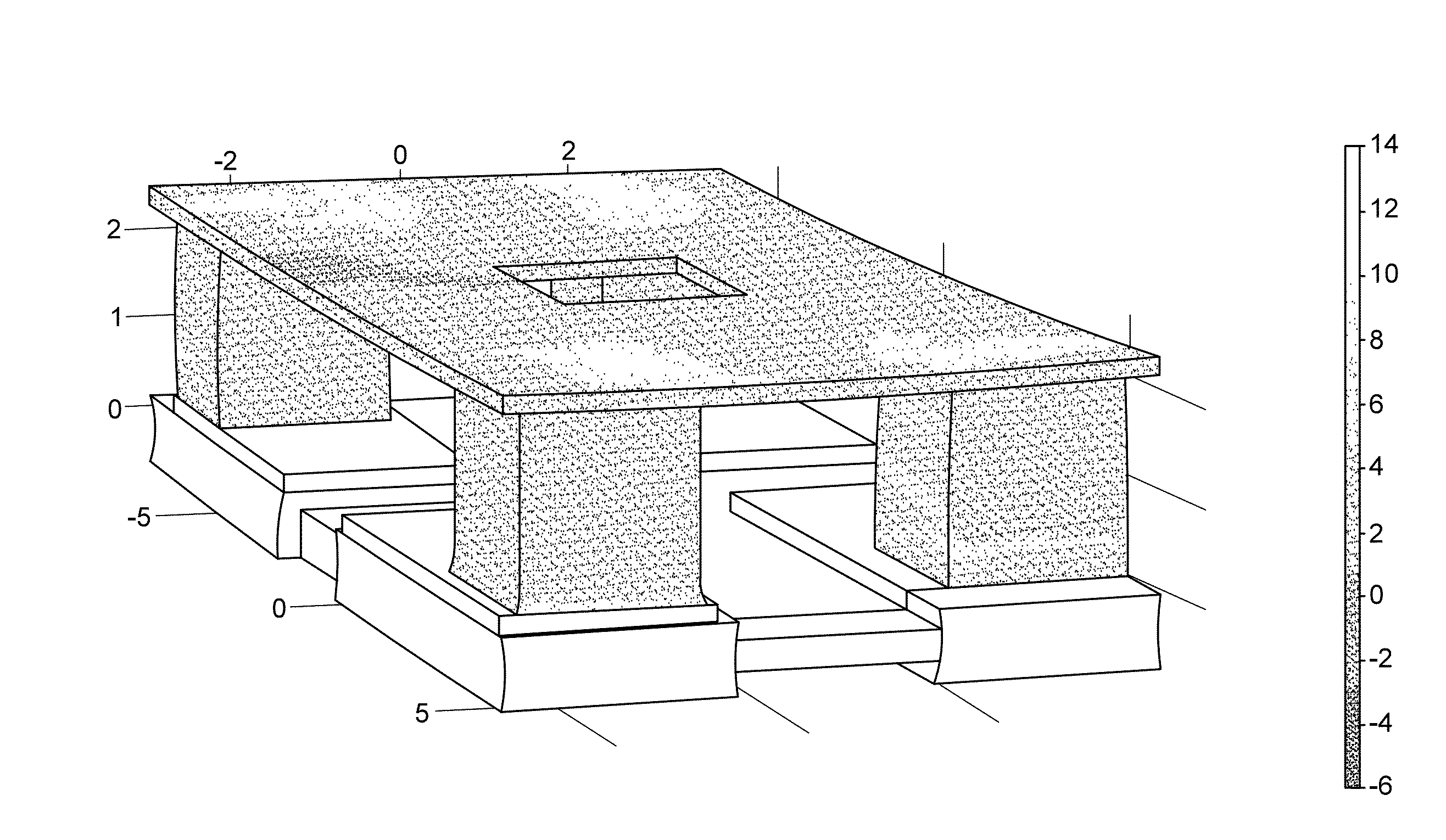
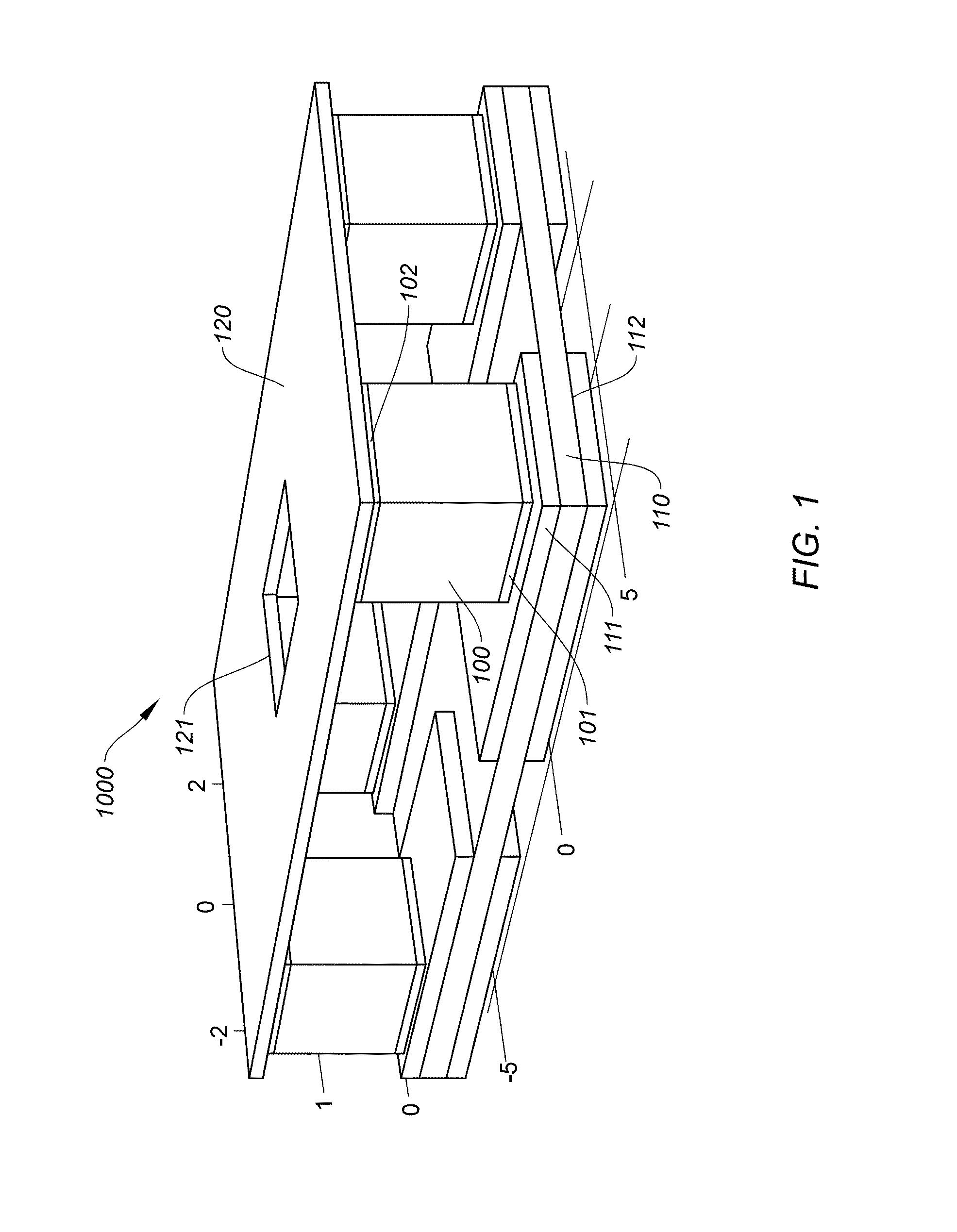
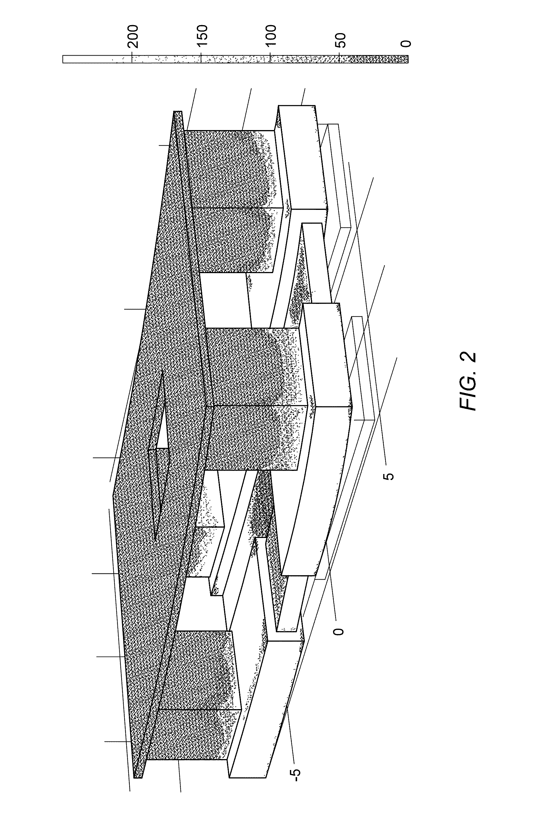
[0026]The present invention is directed to structure and method of thermoelectric device package according to certain embodiments. More particularly, some embodiments of the invention provides structure and method for reducing thermal stresses in thermoelectric legs during manufacturing of a thermoelectric device. Merely by way of example, it has been applied for using CTE (coefficient of thermal expansion) matching ductile materials at the interface between thermoelectric materials and shunts on ceramic base plate. It would be recognized that the invention has a much broader range of applicability.

[0027]Additionally, the present invention is directed to thermoelectric composite structures and methods of making the same according to some embodiments. More particularly, certain embodiments of the invention provide a bulk thermoelectric composite material capped with two metal layers forming a structure for the manufacture and assembly of thermoelectric elements for large-scale thermo...


PUM


Abstract

A method includes preparing a thermoelectric material including p-type or n-type material and first and second caps including transition metal(s). A powder precursor of the first cap can be loaded into a sintering die, punches assembled thereto, and a pre-load applied to form a first pre-pressed structure including a first flat surface. A punch can be removed, a powder precursor of the p-type or n-type material loaded onto that surface, the punch assembled to the die, and a second pre-load applied to form a second pre-pressed structure including a second substantially flat surface. The punch can be removed, a powder precursor of the second cap loaded onto that surface, the first punch assembled to the die, and a third pre-load applied to form a third pre-pressed structure. The third pre-pressed structure can be sintered to form the thermoelectric material; the first or second cap can be coupled to an electrical connector.

Description

CROSS-REFERENCE TO RELATED APPLICATIONS[0001]This application claims priority to the following applications, the entire contents of both of which are incorporated by reference herein:[0002]U.S. Provisional Patent Application No. 61 / 872,745, filed Sep. 1, 2013 and entitled “Thermal Stress and CTE Mismatch Management in Thermoelectric Package;” and[0003]U.S. Provisional Patent Application No. 61 / 955,323, filed Mar. 19, 2014 and entitled “Bulk Metal-Capped Thermoelectric-Composite Sandwich Structure and Method Thereof.”BACKGROUND[0004]The present invention is directed to structure and method of thermoelectric device package according to certain embodiments. More particularly, some embodiments of the invention provide structure and method for reducing thermal stresses in thermoelectric legs during manufacturing a thermoelectric device. Merely by way of example, it has been applied for using CTE (coefficient of thermal expansion) matching ductile materials at the interface between thermo...

Claims


Application Information

Patent Timeline
Patent Type & Authority Applications(United States)
IPC IPC(8): H01L35/34H01L35/22
CPCH01L35/22H01L35/34H10N10/81H10N10/855H10N10/01
Inventor REIFENBERG, JOHNMILLER, LINDSAYSCULLIN, MATTHEW L.LORIMER, ADAMSURA, SRAVAN KUMAR R.BEERA, SASI BHUSHANCRANE, DOUGLAS
Owner ALPHABET ENERGY
Why Eureka
Try Eureka