Self biased dual mode differential CMOS tia for 400g fiber optic links

a fiber optic link and dual-mode technology, applied in the field of communication systems and integrated circuit devices, can solve the problems of increasing and reducing the sensitivity of systems, so as to reduce the cost of modules, the effect of increasing the complexity of systems

Active Publication Date: 2015-03-26
MARVELL ASIA PTE LTD
View PDF8 Cites 22 Cited by
  • Summary
  • Abstract
  • Description
  • Claims
  • Application Information

AI Technical Summary

Benefits of technology

[0007]Future 1 THz and 400 GHz Optical Fiber Links will have multiple channels with 28G and 10G Optical Receivers (Rx) on a single silicon chip implemented in a high-speed deep-submicron CMOS technology. As CMOS technology is scaled down to make circuits and systems run at higher speed and occupy smaller chip (die) area, the operating supply voltage is reduced for lower power. Conventional FET transistors in deep-submicron CMOS processes have very low breakdown voltage, as a result the operating supply voltage is maintained around 1 Volt. The Photo-detectors (PD) used in 28G and 10G Optical Receivers require a bias voltage of more than 2 Volts across the anode and cathode nodes of the PD for better photo-current responsivity.
[0011]Typically, in existing high speed TIA's the PD is AC-coupled to the trans-impedance amplifier (TIA) and / or external voltage is used to bias the PD. AC-coupling between PD and TIA reduces the system sensitivity. Moreover, with multiple channels (over 50 channels in conventional embodiments) the external bias circuits add to the system complexity and increases the module cost. Embodiments of the present invention eliminate the need of external bias circuits and all bias voltages to the PD will be internally generated by the CMOS TIA. Additionally, the architecture described here AC-couples the PD to the TIA reducing noise and improving sensitivity.
[0012]Many benefits are recognized through various embodiments of the present invention. Such benefits include having low inductance radio frequency (RF) return, improved receiver stability, and signal integrity. These benefits can enable higher Zt designs of communications IC chip devices with improved RX sensitivity, or receive sensitivity. In a specific embodiment, the differential approach offers a 1.5 dB SNR improvement. Being in a differential configuration also offers common mode rejection (if such a signal is present) and can also enhance linearity as differential architectures allow for even order harmonic suppression. Other benefits will be recognized by those of ordinary skill in the art that the mechanisms described can be applied to other communications systems as well.

Problems solved by technology

In the early days Internet, popular applications were limited to emails, bulletin board, and mostly informational and text-based web page surfing, and the amount of data transferred was usually relatively small.
Today, Internet and mobile applications demand a huge amount of bandwidth for transferring photo, video, music, and other multimedia files.
These limitations provide significant challenges to the continued improvement of communication systems scaling and performance.
Unfortunately, they have been inadequate for various applications.

Method used


Image

  • Self biased dual mode differential CMOS tia for 400g fiber optic links
  • Self biased dual mode differential CMOS tia for 400g fiber optic links
  • Self biased dual mode differential CMOS tia for 400g fiber optic links

Examples


Embodiment Construction

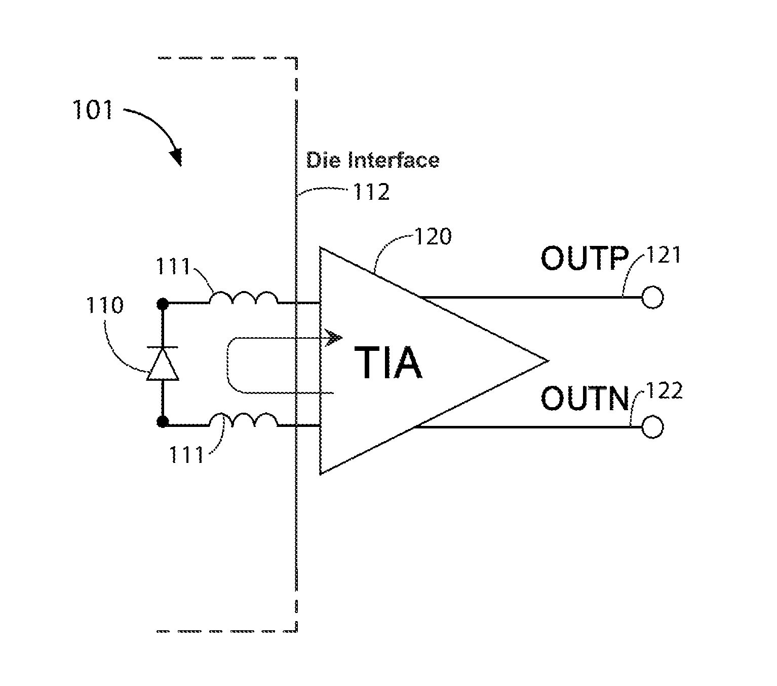
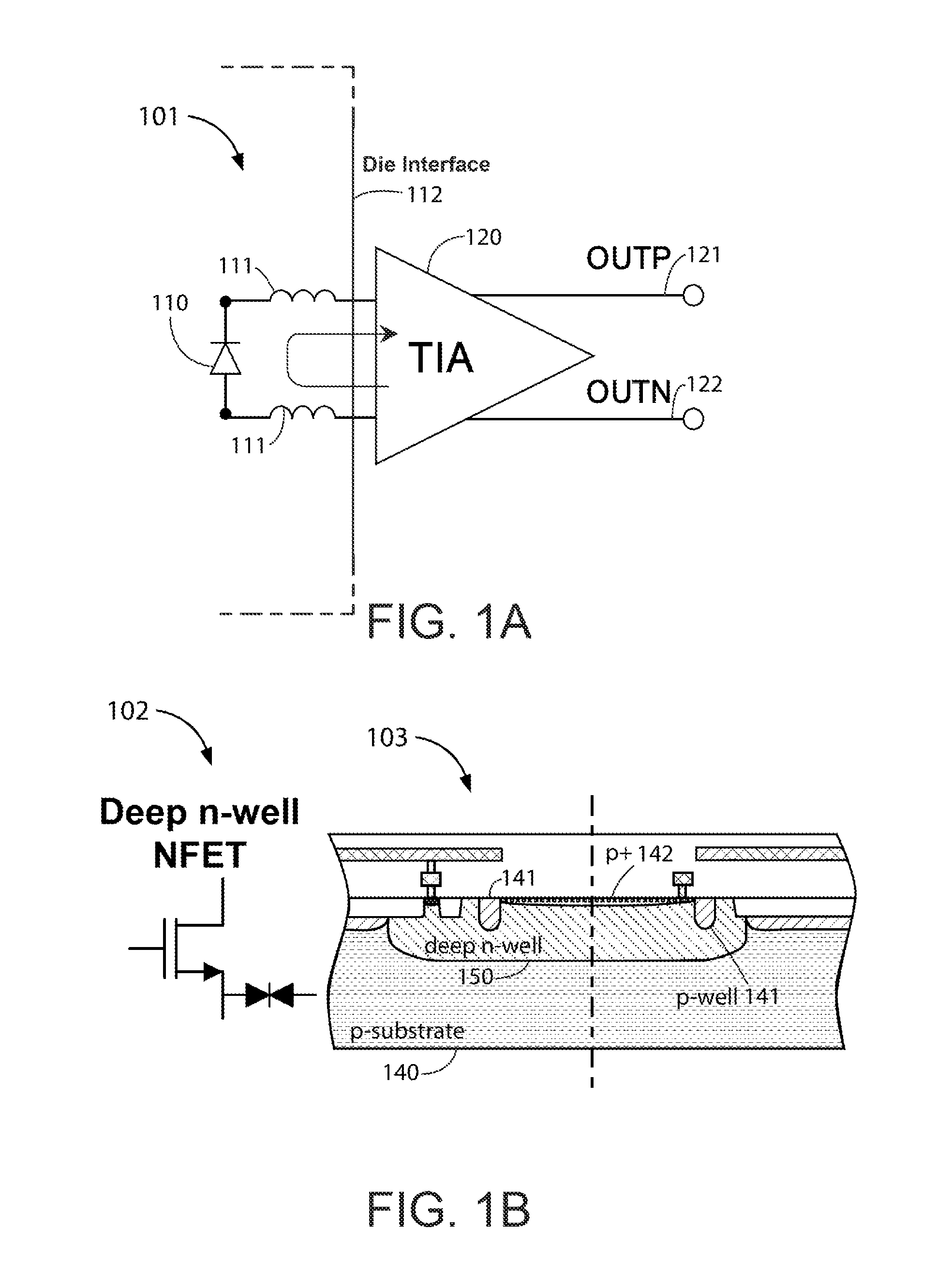
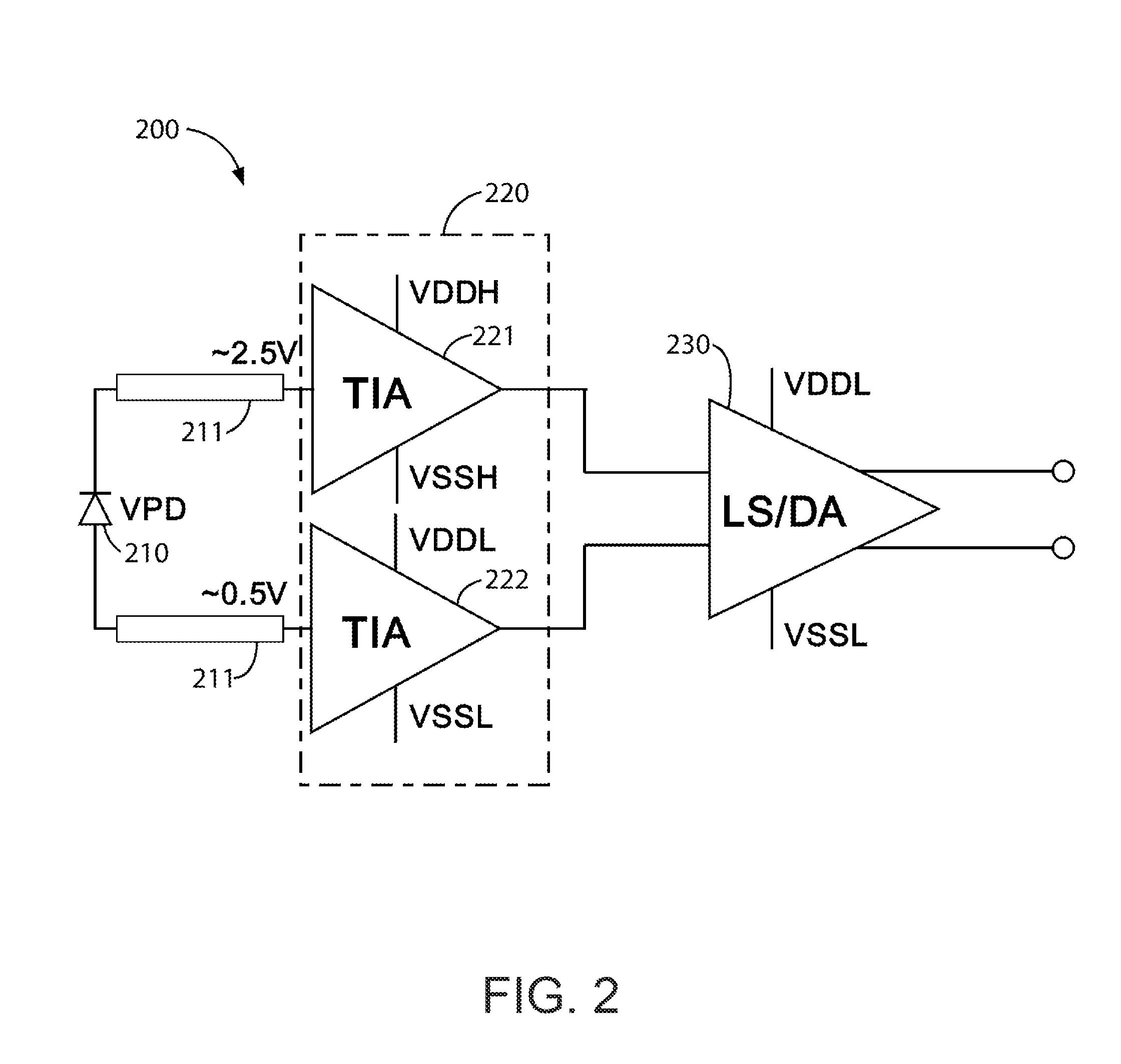
[0027]The present invention is directed to transimpedance amplifier (TIA) devices and systems configured on a single integrated circuit (IC) chip device. More specifically, various embodiments of the present invention provide a self-biased transimpedance amplifier (TIA) device.

[0028]The following description is presented to enable one of ordinary skill in the art to make and use the invention and to incorporate it in the context of particular applications. Various modifications, as well as a variety of uses in different applications will be readily apparent to those skilled in the art, and the general principles defined herein may be applied to a wide range of embodiments. Thus, the present invention is not intended to be limited to the embodiments presented, but is to be accorded the widest scope consistent with the principles and novel features disclosed herein.

[0029]In the following detailed description, numerous specific details are set forth in order to provide a more thorough ...


PUM


Abstract

A transimpedance amplifier (TIA) device. The device includes a photodiode coupled to a differential TIA with a first and second TIA, which is followed by a Level Shifting / Differential Amplifier (LS / DA). The photodiode is coupled between a first and a second input terminal of the first and second TIAs, respectively. The LS / DA can be coupled to a first and second output terminal of the first and second TIAs, respectively. The TIA device includes a semiconductor substrate comprising a plurality of CMOS cells, which can be configured using 28 nm process technology to the first and second TIAs. Each of the CMOS cells can include a deep n-type well region. The second TIA can be configured using a plurality CMOS cells such that the second input terminal is operable at any positive voltage level with respect to an applied voltage to a deep n-well for each of the plurality of second CMOS cells.

Description

CROSS-REFERENCES TO RELATED APPLICATIONS[0001]The present application claims priority to and incorporates by reference, for all purposes, the following provisional application: U.S. Provisional App. 61 / 882,576, filed Sep. 25, 2013.BACKGROUND OF THE INVENTION[0002]The present invention relates to communication systems and integrated circuit (IC) devices. More particularly, the present invention provides an integrated transimpedance amplifier device and method therefor.[0003]Over the last few decades, the use of communication networks exploded. In the early days Internet, popular applications were limited to emails, bulletin board, and mostly informational and text-based web page surfing, and the amount of data transferred was usually relatively small. Today, Internet and mobile applications demand a huge amount of bandwidth for transferring photo, video, music, and other multimedia files. For example, a social network like Facebook processes more than 500 TB of data daily. With such ...

Claims


Application Information

Patent Timeline
Patent Type & Authority Applications(United States)
IPC IPC(8): H03F3/45H04B10/61H03F3/08
CPCH03F3/45179H03F2003/45008H04B10/616H03F3/082H03F3/087H03F3/45475H04B10/693H03F1/0205H03F2200/555
Inventor SHRINGARPURE, RAHULBROEKAERT, TOM PETER EDWARDMAHAJAN, GAURAV
Owner MARVELL ASIA PTE LTD
Why Eureka
Try Eureka