High-frequency semiconductor device and method of manufacturing the same

a semiconductor and high-frequency technology, applied in semiconductor/solid-state device details, capacitors, inductances, etc., can solve the problems of reducing the capacity of the substrate, reducing the density of the transistor, and lowering the strength of the substrate, so as to prevent thermal destruction, and improve the high-frequency characteristics

Active Publication Date: 2015-05-21
SONY CORP +1
View PDF0 Cites 32 Cited by
  • Summary
  • Abstract
  • Description
  • Claims
  • Application Information

AI Technical Summary

Benefits of technology

[0031]In general, as a support substrate of an SOI substrate used for a high-frequency switch, a significantly high resistance substrate is used. Therefore, it is less likely to obtain effects of fixing a substrate electric potential.
[0041]According to the embodiments of the present disclosed technology, a high-frequency semiconductor device having a device structure that prevents thermal destruction by self-heating of a high-frequency transistor formed on an SOI substrate and that has favorable harmonic distortion characteristics, and a method of manufacturing a high-frequency semiconductor device to achieve the foregoing device structure are allowed to be provided.

Problems solved by technology

In this case, it is difficult to arrange transistors densely, and lowered substrate strength is inevitable.
However, in the case where the device having the heat release structure is applied to high-frequency application, since the support substrate is in a floating state, carrier change occurs at the time of applying high frequency, which causes a change in a capacity of the substrate, resulting in lowered high-frequency distortion characteristics.

Method used


Image

  • High-frequency semiconductor device and method of manufacturing the same
  • High-frequency semiconductor device and method of manufacturing the same
  • High-frequency semiconductor device and method of manufacturing the same

Examples


fourth embodiment

4. an embodiment in which a die attachment sheet is provided instead of the support substrate.

5. Fifth Embodiment: an embodiment to demonstrate that a semiconductor substrate itself may be omitted since the support substrate exists in the foregoing first embodiment to the foregoing fourth embodiment.

6. Consideration of appropriate ranges of thicknesses of a doped epitaxial polysilicon layer and a second insulating layer is described.

7. An application example is described.

first embodiment

1. First Embodiment

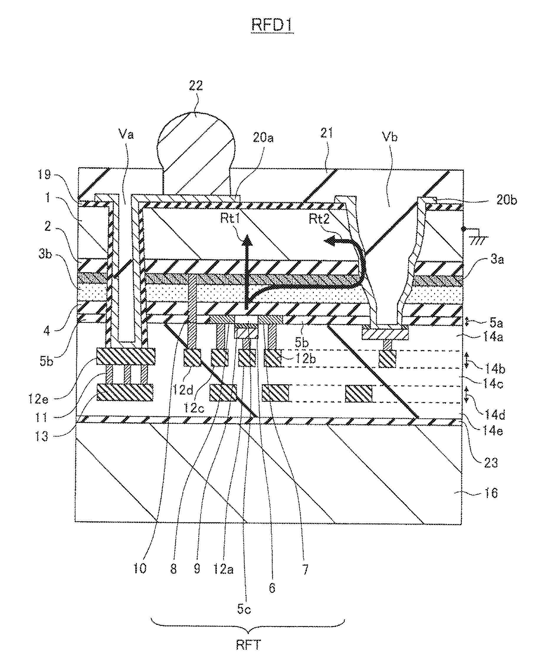
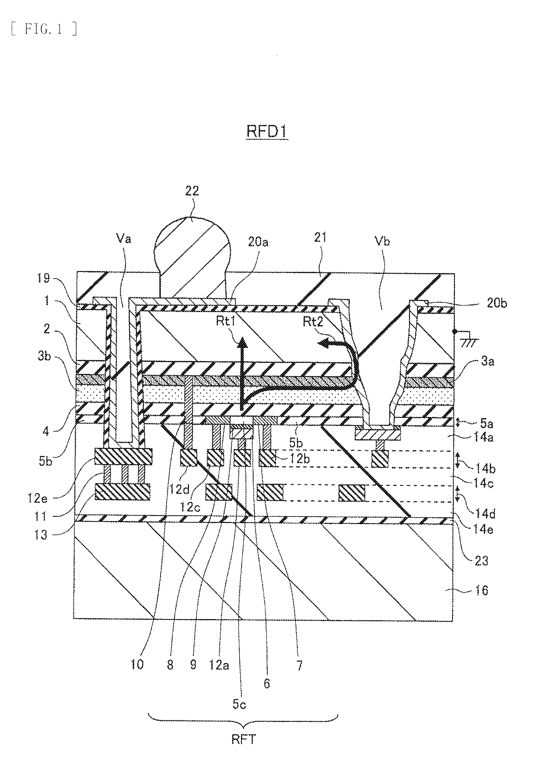
[0099]FIG. 1 illustrates a schematic cross-sectional view of a main section of a high-frequency semiconductor device according to a first embodiment of the present disclosed technology.

[0100]A high-frequency semiconductor device RFD1 illustrated in FIG. 1 has a basic substrate structure in which a semiconductor substrate 1 is bonded to a support substrate 16 with an adhesive 23.

[0101]Various layers and various films are formed on a surface (a first surface) on the support substrate 16 side of the semiconductor substrate 1. Out thereof, a high-frequency transistor RFT is formed in a region centering on a semiconductor layer 5a.

[0102]First, description will be given in more detail of layers laminated on the first surface (the bottom surface in FIG. 1) of the semiconductor substrate 1 and the device (the high-frequency transistor).

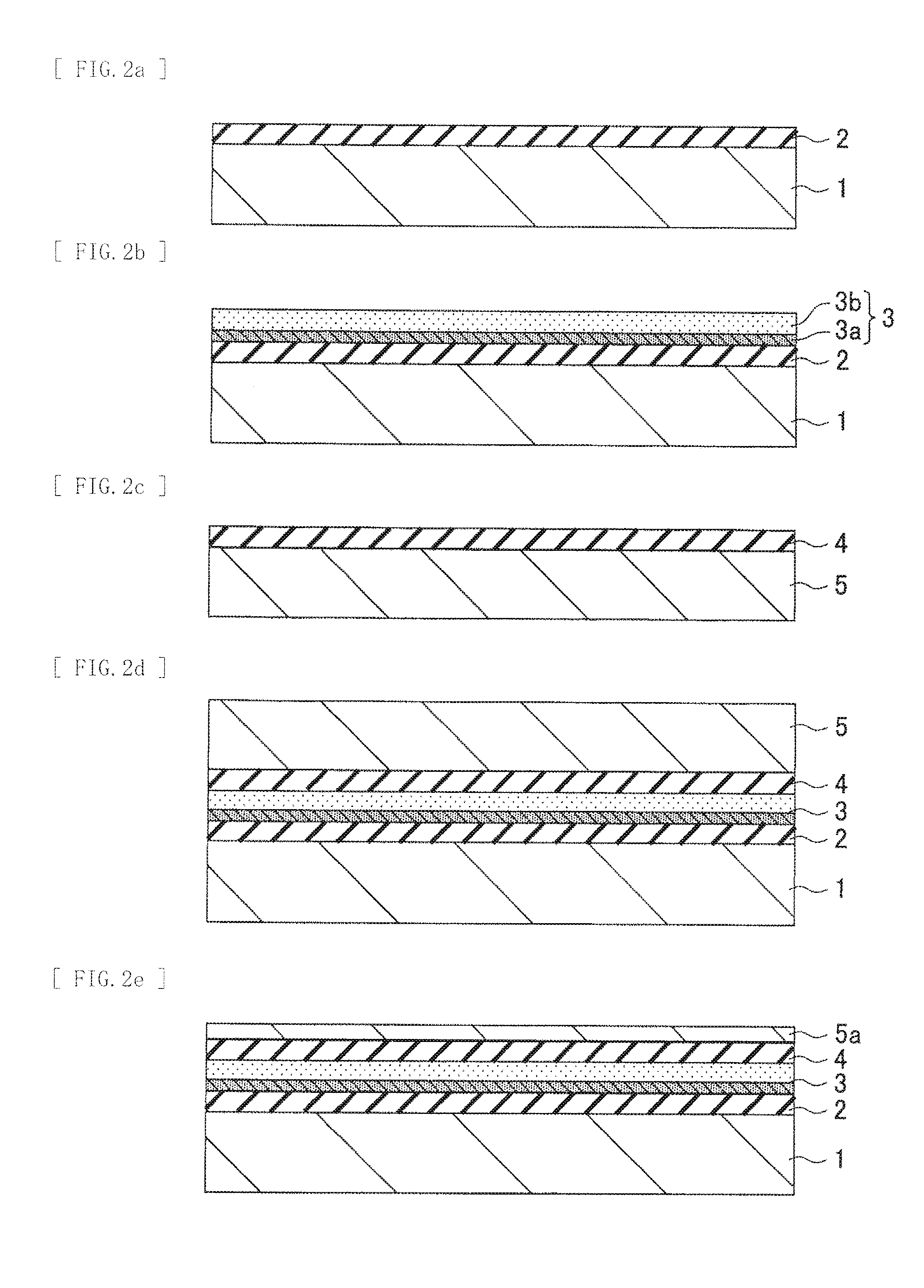
[0103][1.1 Structure of Epitaxial Growth Layer]

[0104]From the first surface (the bottom surface) side of the semiconductor substrate 1, a...

second embodiment

2. Second Embodiment

[0216]FIG. 12 illustrates a cross-sectional view of a main section in this embodiment corresponding to FIG. 1 in a high-frequency semiconductor device RFD 2.

[0217]The high-frequency semiconductor device RFD 2 (FIG. 12) according to this embodiment is different from the high-frequency semiconductor device RFD 1 (FIG. 1) according to the first embodiment in that the high-frequency semiconductor device RFD 2 additionally includes a heat release metal.

[0218]The foregoing heat release metal is also called a “dummy wiring section.” The “dummy wiring section” is different from a wiring layer that is electrically connected directly to the high-frequency transistor RFT or indirectly to the high-frequency transistor RFT through other element as the second wiring layer 14d illustrated in FIG. 1. The “dummy wiring section” refers to an electrically conductive layer that is not connected to other electrically-conductive member used as a wiring of a circuit or an element in it...


PUM


Abstract

A high-frequency semiconductor device, wherein on one surface of a semiconductor substrate, a first insulating layer, an undoped epitaxial polysilicon layer in a state of column crystal, a second insulating layer, and a semiconductor layer are formed in order from a side of the one surface, and a high-frequency transistor is formed in a location of the semiconductor layer facing the undoped epitaxial polysilicon layer with the second insulating layer in between.

Description

TECHNICAL FIELD[0001]The present disclosed technology relates to a high-frequency semiconductor device that includes a high-frequency transistor having a so-called SOI (silicon on insulator)-type element structure and to a method of manufacturing the same.BACKGROUND ART[0002]High-frequency transistors have been widely used for the purpose of, for example, high-frequency signal processing such as signal transmission, signal reception, and switching received signals and the like of wireless communication apparatuses such as a mobile phone and a wireless LAN.[0003]For such a high-frequency transistor, a small coupling capacitance (a small parasitic capacitance) with respect to a substrate is demanded in order to perform high-speed operation.[0004]Therefore, as a high-frequency transistor, an FET (field-effect transistor) of a compound semiconductor such as GaAs with low electric power consumption capable of simply forming a complicated circuit has been often used for a long time.[0005]...

Claims


Application Information

Patent Timeline
Patent Type & Authority Applications(United States)
IPC IPC(8): H01L29/78H01L21/768H01L23/522
CPCH01L29/78H01L21/768H01L23/522H01L21/76898H01L23/481H01L23/5223H01L23/5227H01L23/5228H01L24/11H01L27/12H01L27/13H01L28/10H01L28/24H01L28/40H01L2924/07802H01L2924/13091H01L2924/1306H01L2924/1305H01L2924/00H01L2924/15788H01L21/84H01L29/78606H01L29/78642
Inventor TSUNEMI, HIROKIYAMAGATA, HIDEONAGAI, KENJIIBUSUKI, YUJI
Owner SONY CORP
Why Eureka
Try Eureka