Optical Waveguide Devices

a technology of optical waveguides and thin layers, applied in the direction of optical waveguide light guides, instruments, optics, etc., can solve the problems of poor adhesion of the loaded ridge portion and the thin layer, poor adhesion to the surface of the thin layer, and lowered production yield, so as to prevent peeling, reduce propagation loss, and good adhesion

Active Publication Date: 2015-05-28
NGK INSULATORS LTD
View PDF6 Cites 3 Cited by
  • Summary
  • Abstract
  • Description
  • Claims
  • Application Information

AI Technical Summary

Benefits of technology

[0017]According to the present invention, the shape of the ridge portion can be designed relatively freely, by changing a shape of a patterning mask. It is thereby possible to form a curved or branched, loaded-type optical waveguide.
[0018]Then, since the cross sectional shape of the ridge portion loaded on the thin layer is trapezoidal shape

Problems solved by technology

However, the loaded ridge portion was susceptible to separation from the thin layer so that the production yield was lowered.
As the inventors have studied the cause of the increase of propagation loss, it was proved that the adhesion of the loaded ridge portion and

Method used


Image

  • Optical Waveguide Devices
  • Optical Waveguide Devices
  • Optical Waveguide Devices

Examples


##ventive example 1

Inventive Example 1

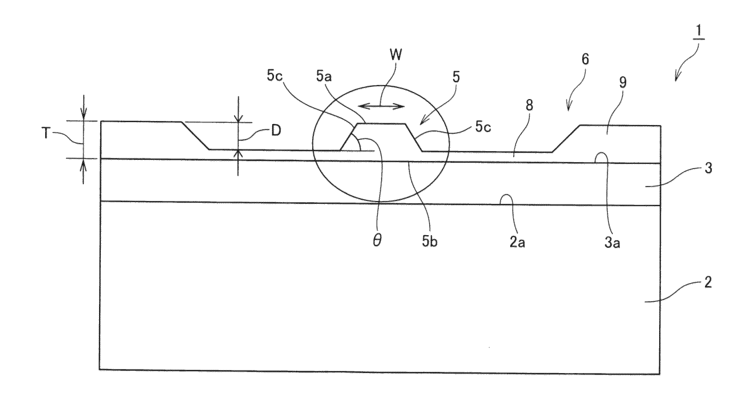
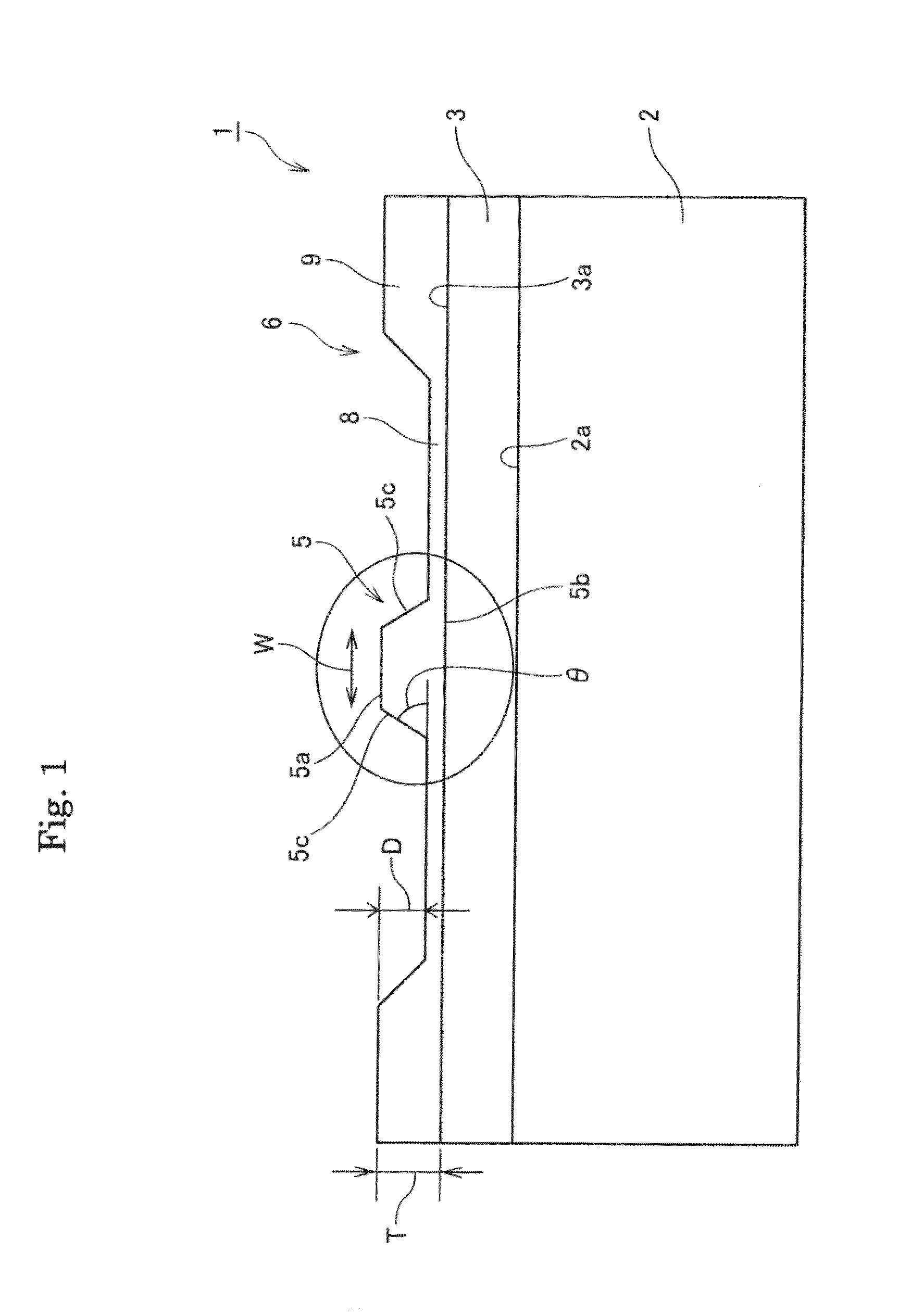
[0072]It was produced the device 1 as described in FIGS. 1, 4(a) and 5.

[0073]Specifically, it was produced a laminated body including the thin layer 3 of MgO-doped lithium niobate (thickness of 2.0 μm), clad layer of SiO2, adhesive layer and supporting body 2 composed of a Y-cut plate made of non-doped lithium niobate and having a thickness of 0.5 mm. A film of Ta2O5 with a thickness of 1.5 μm was formed on the thin layer 3 by sputtering.

[0074]Then, films of molybdenum each having a thickness of 100 nm were formed on the upper face 3a of the thin layer 3 and bottom face of the supporting body 2, respectively. Then, resist patterns were formed on the thin layer and on the molybdenum film, respectively, by photolithography method (application of the resist and development). Further, the resist was applied onto the whole surface of the bottom face of the supporting body 2. The molybdenum film was then subjected to wet etching to remove the resist and to leave a patte...

##ventive example 2

Inventive Example 2

[0088]The device was produced as described in the inventive example 1, except that the material of the thin layer 3 was made MgO-doped lithium tantalate single crystal. As a result, it was obtained the similar result as that in the inventive example 1. Further, as the tape peeling test was performed, the adhesion of the tape onto the film and the peeling of the ridge portion from the device were not observed.

##ventive example 3

Inventive Example 3

[0089]The device was produced as described in the inventive example 1, except that the material of the thin layer 3 was made yttrium vanadate crystal. For confirming the properties of the optical waveguide, the propagation loss was measured at a wavelength of 980 nm as the inventive example 1 to obtain a value of 0.5 dB / cm. Further, as the tape peeling test was performed, the adhesion of the tape onto the film and the peeling of the ridge portion from the device were not observed.


PUM


Abstract

An optical waveguide device 1 includes a thin layer 3 and a ridge portion 5 loaded on the thin layer 3. The thin layer 3 is made of an optical material selected from the group consisting of lithium niobate, lithium tantalate, lithium niobate-lithium tantalate, yttrium aluminum garnet, yttrium vanadate, gadolinium vanadate, potassium gadolinium tungstate; and potassium yttrium tungstate. The ridge portion 5 is made of tantalum pentoxide and has a trapezoid shape viewed in a cross section perpendicular to a direction of propagation of light. The ridge portion is not peeled off from the thin layer in a tape peeling test.

Description

[0001]This application claims the benefit of Japanese Patent Application No. P2013-245782 filed on Nov. 28, 2013, the entirety of which is incorporated by reference.TECHNICAL FIELD[0002]The present invention relates to optical waveguide devices.BACKGROUND ARTS[0003]Nonlinear optical crystal such as lithium niobate or lithium tantalate single crystal has a high secondary nonlinear optical constant. When a periodic domain polarization inversion structure is formed in the above crystals, a second-harmonic-generation (SHG) device of a quasi-phase-matched (QPM) system can be realized. Further, when a waveguide is formed within this periodic domain inversion structure, the high-efficiency SHG device can be realized and further, applied to optical communication, medical science, photochemistry, various optical measurements over a wide range.[0004]Conventionally, it is required a light source of fundamental wave called exiting light from the outside of an SHG device. For example, in the cas...

Claims


Application Information

Patent Timeline
IPC IPC(8): G02B6/10G02F1/35G02B1/10
CPCG02B6/10G02B1/10G02F2001/3509G02F2001/3505G02F1/3501G02B6/122G02B6/125G02B2006/12176G02F1/3503
Inventor ASAI, KEIICHIROYAMAGUCHI, SHOICHIRO
Owner NGK INSULATORS LTD
Why Eureka
Try Eureka