Nitride LED structure with double graded electron blocking layer

a technology of electron blocking layer and led structure, which is applied in the direction of basic electric elements, semiconductor devices, electrical equipment, etc., can solve the problems of low efficiency, low efficiency, and low efficiency, and achieve high efficiency, reduced electron leakage, and high aluminium composition

Inactive Publication Date: 2015-06-25
SHARP KK
View PDF2 Cites 13 Cited by
  • Summary
  • Abstract
  • Description
  • Claims
  • Application Information

AI Technical Summary

Benefits of technology

[0008]In view of the above deficiencies of conventional LEDs, it is an object of the present invention to address the above problems by providing an LED w

Problems solved by technology

However, such LEDs still suffer from degraded performance at high current injection caused by a phenomenon commonly referred to in the art as “efficiency droop”.
It has been reported in the literature that one possible cause of the efficiency droop may be due to the injected electrons leaking out of the active region.
However, making an EBL with large energy band gap, i.e. with high aluminium composition, is difficult to grow with high quality material because of the lattice mismatch between GaN and AlGaN.
The effect of such valence band spike on the efficiency of the carrier recombination is then limited.
Moreover, it is difficult to grow an EBL dir

Method used


Image

  • Nitride LED structure with double graded electron blocking layer
  • Nitride LED structure with double graded electron blocking layer
  • Nitride LED structure with double graded electron blocking layer

Examples


first embodiment

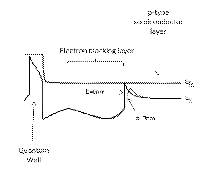
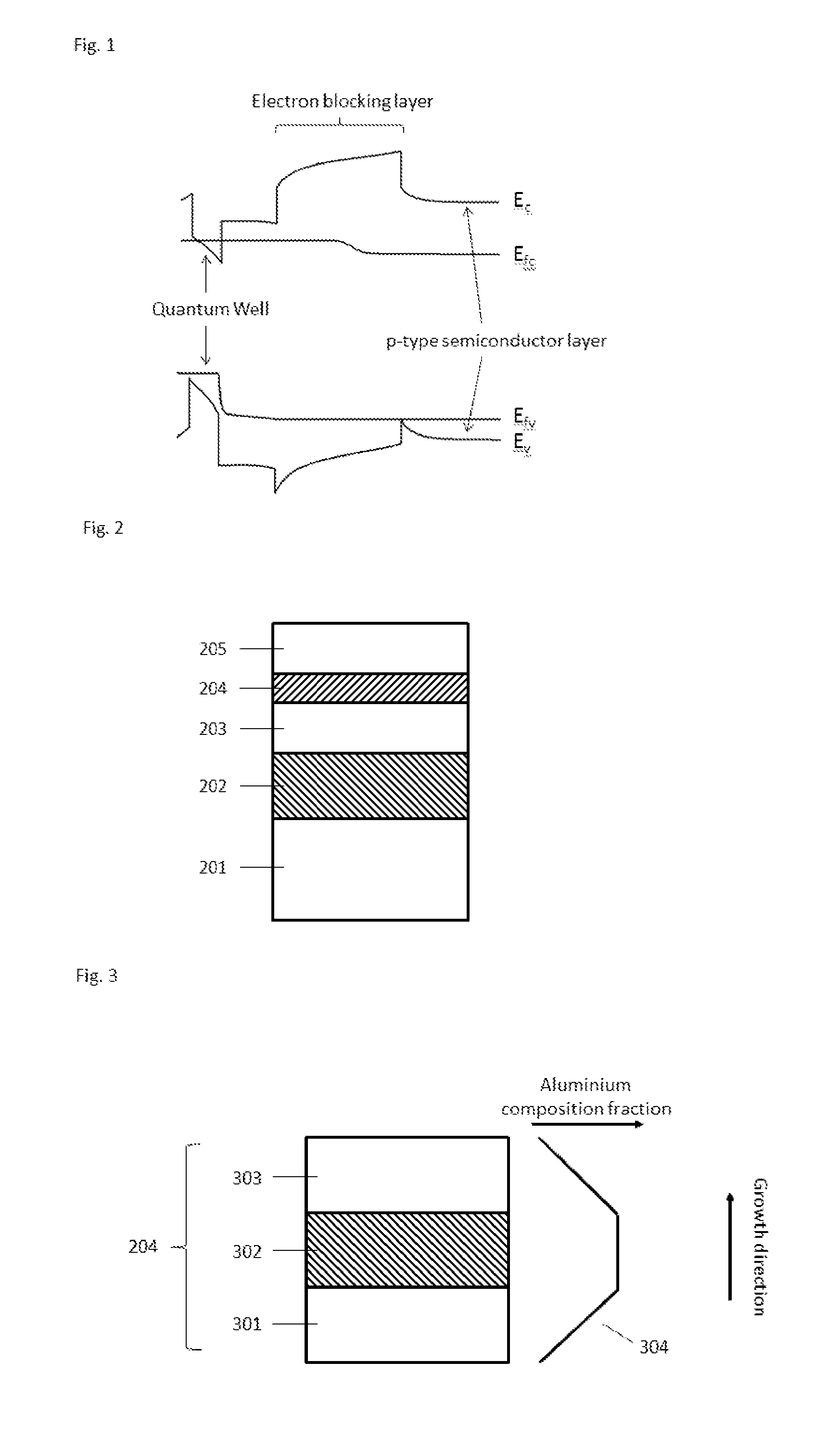
[0036]An example of an electron blocking region 204 with 3 layers according to this invention is represented in FIG. 3, and may contain: a upgraded layer 301, a middle layer 302 disposed on the upgraded layer 301 and a downgraded layer 303 disposed on top of the middle layer 302. Because of the existence of the middle layer 302, the maximum aluminium composition of the electron blocking region under mass production is stabilized.

[0037]In this example, the three layers 301, 302 and 303 of the electron blocking region 204 include, but are not limited to, AlxInyGa1-x-yN wherein 0301, 302 and 303 of the electron blocking region 204 have all the same thickness. However, the three layers 301, 302 and 303 may have different thicknesses.

[0038]The composition of each of the layers of the electron blocking region 204 will be described according to the first embodiment of this invention, with reference to FIG. 3 and to the aluminium composition profile 304 of FIG. 3.

[0039]The upgraded layer 30...

second embodiment

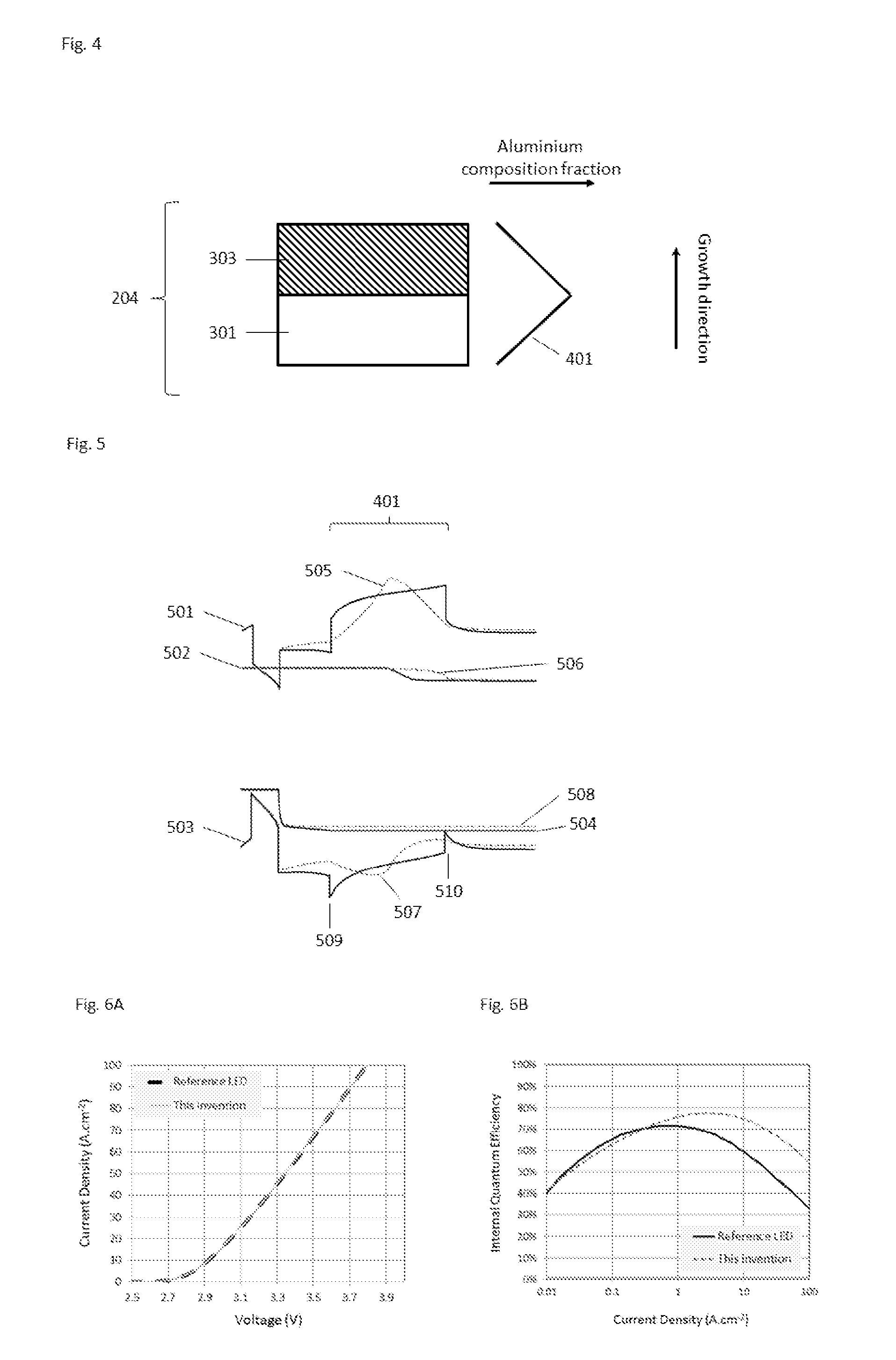
[0044]Such composition profile in each of the layers of the electron blocking region 204 has an effect on the conduction band and valence band profile. FIG. 5 is comparing the simulation results from a reference LED structure which is similar to FIG. 2, wherein the electron blocking region 204 is made of a single layer of AlxGa1-xN, to an LED structure having an electron blocking layer as described in this second embodiment and illustrated in FIG. 4. In this example, the aluminium composition fraction of the electron blocking region of the reference LED is constant at 0.22 and the thickness of the electron blocking region is 18 nm. Also in this example, but not limiting the scope of this invention, the aluminium composition fraction of the upgraded layer 301 of the electron blocking region 204 of the LED related to this invention is linearly graded from 0 to 0.3, and the aluminium composition fraction of the downgraded layer 303 of the electron blocking region is linearly graded fro...

third embodiment

[0063]In the present invention, and as illustrated in FIG. 11 and FIG. 12, the aluminium composition profile of the upgraded 301 and downgraded 303 layers of the electron blocking region 204 can be non-linear. More specifically the gradient of aluminium composition of the upgraded layer 301 and / or the downgraded layer is larger as the aluminium composition increases. The gradient shape can be exponential, logarithmic or polynominal. This structure has an advantage that the low-crystal quality high Al composition region can be smaller.


PUM


Abstract

A group III nitride-based light emitting device includes an n-type semiconductor layer; a first p-type semiconductor layer; an active region; and an electron blocking region comprising AlGaInN located between the active region and the first p-type semiconductor layer, and including at least an upgraded layer and a downgraded layer. An aluminium composition of the upgraded layer of the electron blocking region increases from an active region side to a first p-type semiconductor layer side of the electron blocking region, and an aluminium composition of the downgraded layer of the electron blocking region decreases from the active region side to the first p-type semiconductor layer side of the electron blocking region. The nitride-based light emitting device may be a light emitting diode or a laser diode.

Description

TECHNICAL FIELD[0001]The present invention relates to the field of light emitting devices, and more particularly to the improvement of the light output efficiency of a light emitting device.BACKGROUND OF THE INVENTION[0002]Light emitting diodes (LEDs) are key components to a wide range of applications that include backlighting units for liquid crystal displays, headlamps for automobiles, or general lighting. For example, III-nitride semiconductor based blue and green emitting LEDs are widely used in these applications. However, such LEDs still suffer from degraded performance at high current injection caused by a phenomenon commonly referred to in the art as “efficiency droop”.[0003]A standard LED structure includes an electron supply layer (e.g. generally n-type semiconductor), a hole supply layer (e.g. p-type semiconductor) and an active region (e.g. light emitting area which can include single or multiple quantum wells). A multiple quantum well structure includes quantum wells an...

Claims


Application Information

Patent Timeline
IPC IPC(8): H01L33/14H01L33/00
CPCH01L33/0025H01L33/145H01L33/06H01L33/32
Inventor SENES, MATHIEUTAKEOKA, TADASHI
Owner SHARP KK
Why Eureka
Try Eureka