Depositing Calcium Fluoride Template Layers for Solar Cells

a solar cell and template layer technology, applied in applications, other domestic articles, transportation and packaging, etc., can solve the problems of limiting the potential silicon pv cost reduction, high recombination rate than low angle grain boundaries, and high cost of silicon wafer fabrication and energy consumption

Active Publication Date: 2015-07-16
THE BOARD OF TRUSTEES OF THE LELAND STANFORD JUNIOR UNIV
View PDF3 Cites 5 Cited by
  • Summary
  • Abstract
  • Description
  • Claims
  • Application Information

AI Technical Summary

Problems solved by technology

In particular, the high dislocation density of high-angle grain boundaries result in a higher recombination rate than low angle grain boundaries.
Both types of misorientation result in defect densities that lead to recombination.
However, silicon wafer fabrication is expensive and energy intensive, limiting potential silicon PV cost reductions.
Such inexpensive substrates (e.g. display glass) are generally amorphous or polycrystalline and cannot sustain high temperatures for long periods; therefore, it is difficult to grow high quality c-Si on them.
Furthermore, grain boundaries parallel to the surface may impede hydrogen diffusion into the film, reducing the efficacy of post-growth hydrogenation treatments.
Although solar cells made from silicon wafers dominate the existing photovoltaic (PV) market, the wafer fabrication process is energy-intensive and expensive, comprising about half of the typical module price.

Method used


Image

  • Depositing Calcium Fluoride Template Layers for Solar Cells
  • Depositing Calcium Fluoride Template Layers for Solar Cells
  • Depositing Calcium Fluoride Template Layers for Solar Cells

Examples


Embodiment Construction

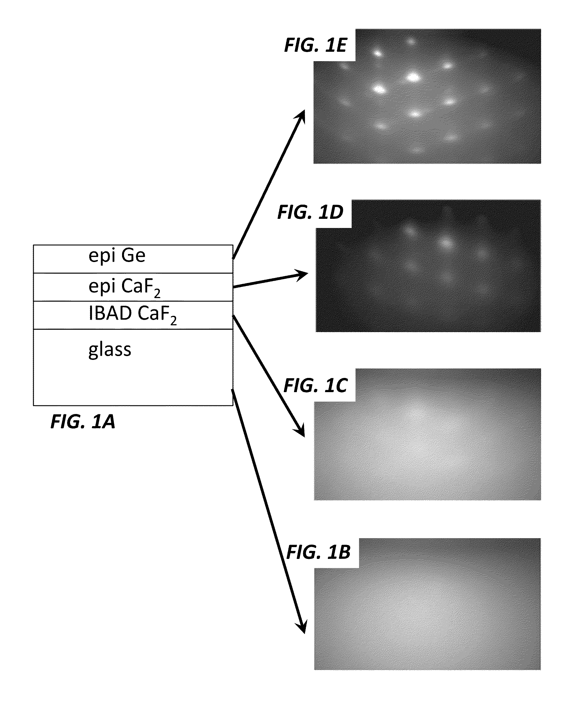
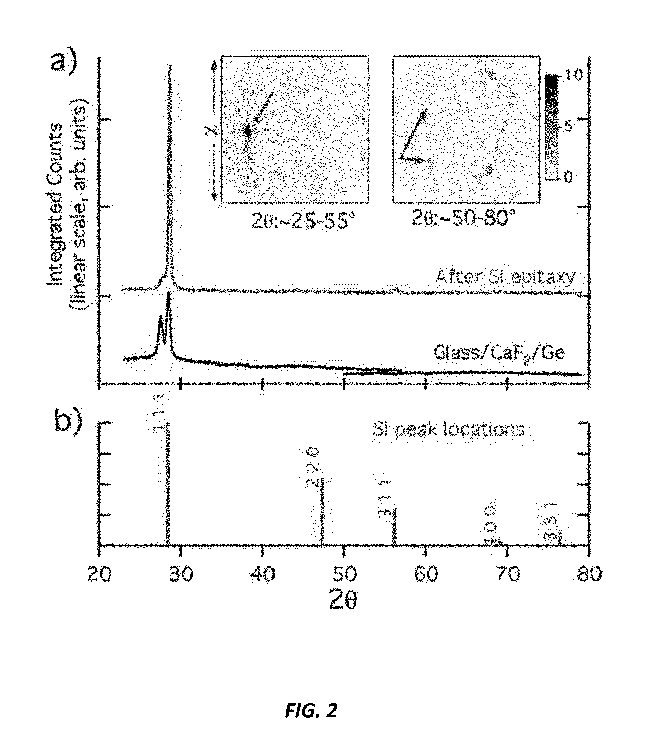
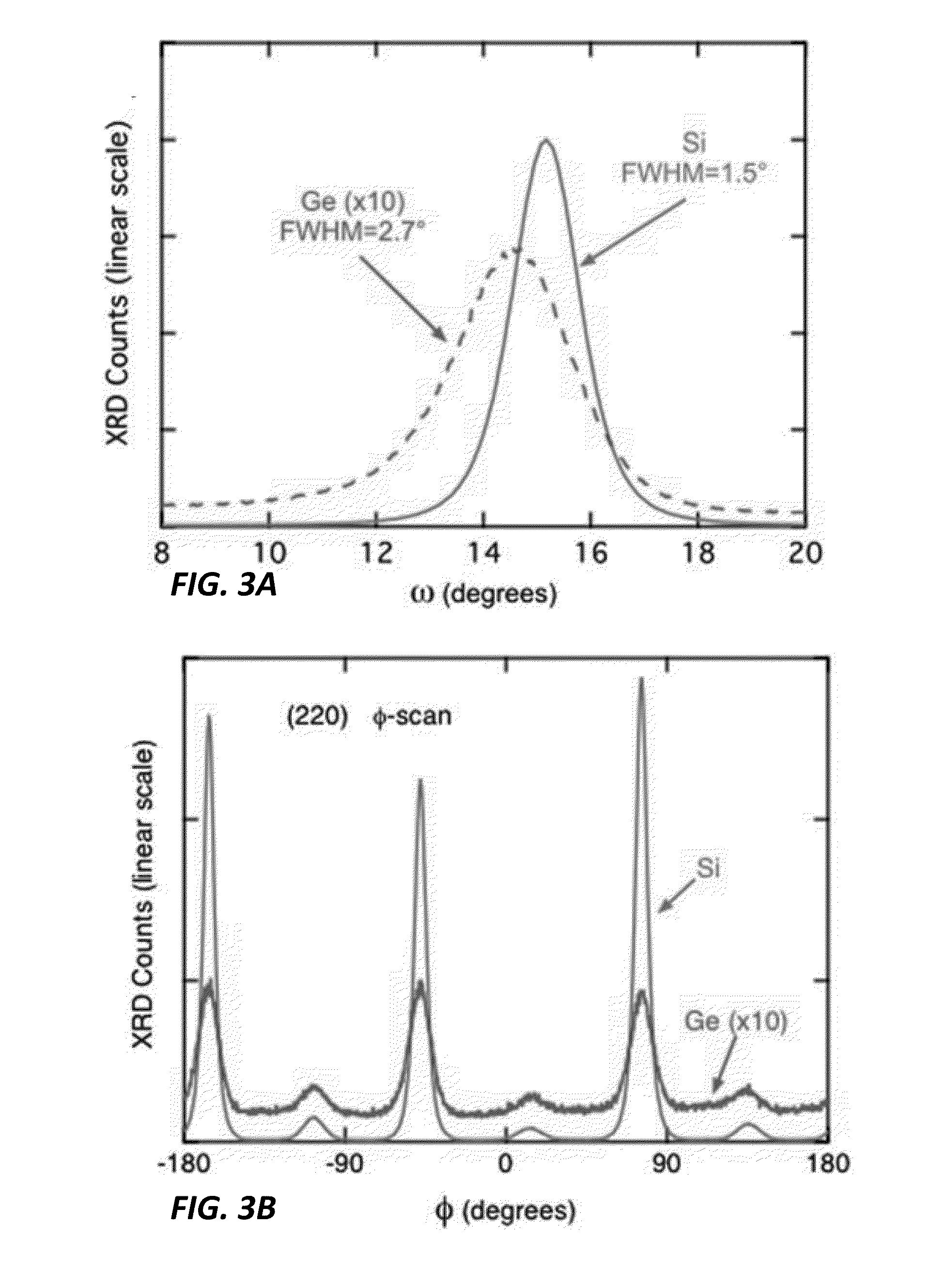
[0029]Ion beam assisted deposition is a proven technology for growing thin films with biaxial texture, similar to single crystals. In one embodiment, the invention provides a PV device and a method to control the grain boundary alignment in a polycrystalline thin film of silicon. This is achieved by depositing a biaxially aligned layer of calcium fluoride (CaF2) or yttrium oxide-stabilized zirconium oxide (YSZ) that can be used as a template layer for the subsequent deposition of epitaxial layers. The biaxial alignment of the template layer is achieved by using the ion beam assisted deposition process (IBAD). The IBAD template layer can then be used as a platform for subsequent deposition of heteroepitaxial silicon or other materials. This invention enables the deposition of polycrystalline silicon on technical substrates of large areas or long lengths. The invention may be used to deposit polycrystalline silicon on large areas for photovoltaic applications. The technology can be ap...


PUM

PropertyMeasurementUnit
lattice constantaaaaaaaaaa
grain widthsaaaaaaaaaa

Abstract

A biaxially textured crystalline layer formed on a substrate using ion beam assisted deposition (IBAD) is provided. The biaxially textured crystalline layer includes an oriented CaF2 crystalline layer having crystalline grains oriented in both in-plane and out-of-plane directions, where the out-of-plane orientation is a (111) out-of-plane orientation. The oriented CaF2 crystalline layer is disposed for growth of a subsequent epitaxial layer and the CaF2 crystalline layer is an IBAD CaF2 layer. The biaxially textured CaF2 layer can be used in a photovoltaic cell, an electronic or optoelectronic device, an integrated circuit, an optical sensor, or a magnetic device.

Description

CROSS-REFERENCE TO RELATED APPLICATIONS[0001]This application is a continuation of U.S. patent application Ser. No. 13 / 442,658 filed Apr. 9, 2012, which is incorporated herein by reference. U.S. patent application Ser. No. 13 / 442,648 claims priority from U.S. Provisional Patent Application 61 / 516,834 filed Apr. 8, 2011, which is incorporated herein by reference.FIELD OF THE INVENTION[0002]The present invention relates generally to biaxially oriented, polycrystalline thin films. More particularly, the invention relates to a method for forming biaxially oriented CaF2 with a (111) biaxial texture for crystallographically oriented silicon solar cells.BACKGROUND OF THE INVENTION[0003]Solar cell efficiency is a strong function of minority carrier lifetime, since photo-generated carriers that recombine before reaching the p-n junction do not contribute to photocurrent. Grain boundaries in polycrystalline silicon films provide electron traps that act as recombination centers that reduce min...

Claims


Application Information

Patent Timeline
Patent Type & Authority Applications(United States)
IPC IPC(8): C23C14/06C23C14/22
CPCC23C14/221C23C14/0694B32B7/02B32B2307/704B32B2457/00Y10T428/24355C30B25/06
Inventor CLEMENS, BRUCE M.GROVES, JAMES R.HAYES, GARRETT J.LI, BINGRUI JOELSALLEO, ALBERTO
Owner THE BOARD OF TRUSTEES OF THE LELAND STANFORD JUNIOR UNIV
Why Eureka
Try Eureka