Method and structure to enhance gate induced strain effect in multigate device

a multi-gate device and gate induced strain technology, applied in the field of semiconductor device manufacturing, can solve the problems of increasing the difficulty of meeting the transistor drive current performance, significantly reducing the stressor volume, so as to increase the mobility and drive current

Active Publication Date: 2015-07-23
IBM CORP
View PDF0 Cites 31 Cited by
  • Summary
  • Abstract
  • Description
  • Claims
  • Application Information

AI Technical Summary

Benefits of technology

[0009]In one aspect, embodiments of the invention provide a method and a FinFET device structure that form a gate stack stress of a finFET to increase the mobility and drive current.
[0010]In an embodiment, a method is described of forming a FinFET that includes depositing high-k dielectric on a patterned fin structure with recess shallow trench isolation. A workfunction metal and a very thin layer of poly crystalline silicon are then deposited on top of the high-k materials. A stress containing material such as high Ge percentage silicon germanium film and / or highly stress W film is then deposited on top of the poly crystalline silicon film. In the case of a high Ge percentage silicon film, the film can be formed either in-situ or ex-situ doped with dopant to lower the gate resistance. The in-situ doped film can be achieved by incorporating dopants during the silicon germanium epitaxial growth, whereas the ex-situ doped film can be achieved by ion-implantation following a silicon germanium epitaxial growth. Preferably, the gate stack has thick poly-crystalline silicon on top of the workfunction metal that occupies the space between the fins, leaving no room for strain producing material to impart a stress in the transistor channel for mobility enhancement.
[0011]In an embodiment, a method and structure are described freeing up the space between the fins to allow the stressor films being deposited closer to the channel, thus improving the proximity of the stress containing material to the transistor channel, thereby enhancing the stress coupling efficiency defined as the ratio between the stress level in the stressor film and the stress transferred to the channel for mobility enhancement.

Problems solved by technology

As the device continues to the nanometer scaling, the requirement for the transistor drive current performance becomes increasingly more difficult to meet.
One difficulty that encountered resides in the conventional stress effect, such as an embedded silicon germanium, embedded silicon carbon source drain, and dual stress silicon nitride liner set to boost the carrier mobility that diminishes significantly with the scaling of the gate contact pitch.
However, because of the pitch scaling, the available space for the source and drain stressor formation becoming smaller and smaller, this leading to the decrease of the stressor volume and a greatly reduction of the stress effect from the source and the drain region.
Another factor that limits the usage of source and drain extrinsic stressor is the transition from the planar device structure to the FinFFT type of the transistor structure.
The reduction of the aforementioned two effects (stressor volume and stress coupling) makes the stress engineering of the FinFET device structure ever more challenging compared to that of previous generations.
The challenge for the gate induced strain, however, is how to implement it through the selection of gate stack materials to meet not only the channel strain requirement for carrier mobility boost, but also a workfunction setting to meet the transistor threshold voltage requirement.
Notably, a highly stress W would fail to achieve the same results.

Method used


Image

  • Method and structure to enhance gate induced strain effect in multigate device
  • Method and structure to enhance gate induced strain effect in multigate device
  • Method and structure to enhance gate induced strain effect in multigate device

Examples


Embodiment Construction

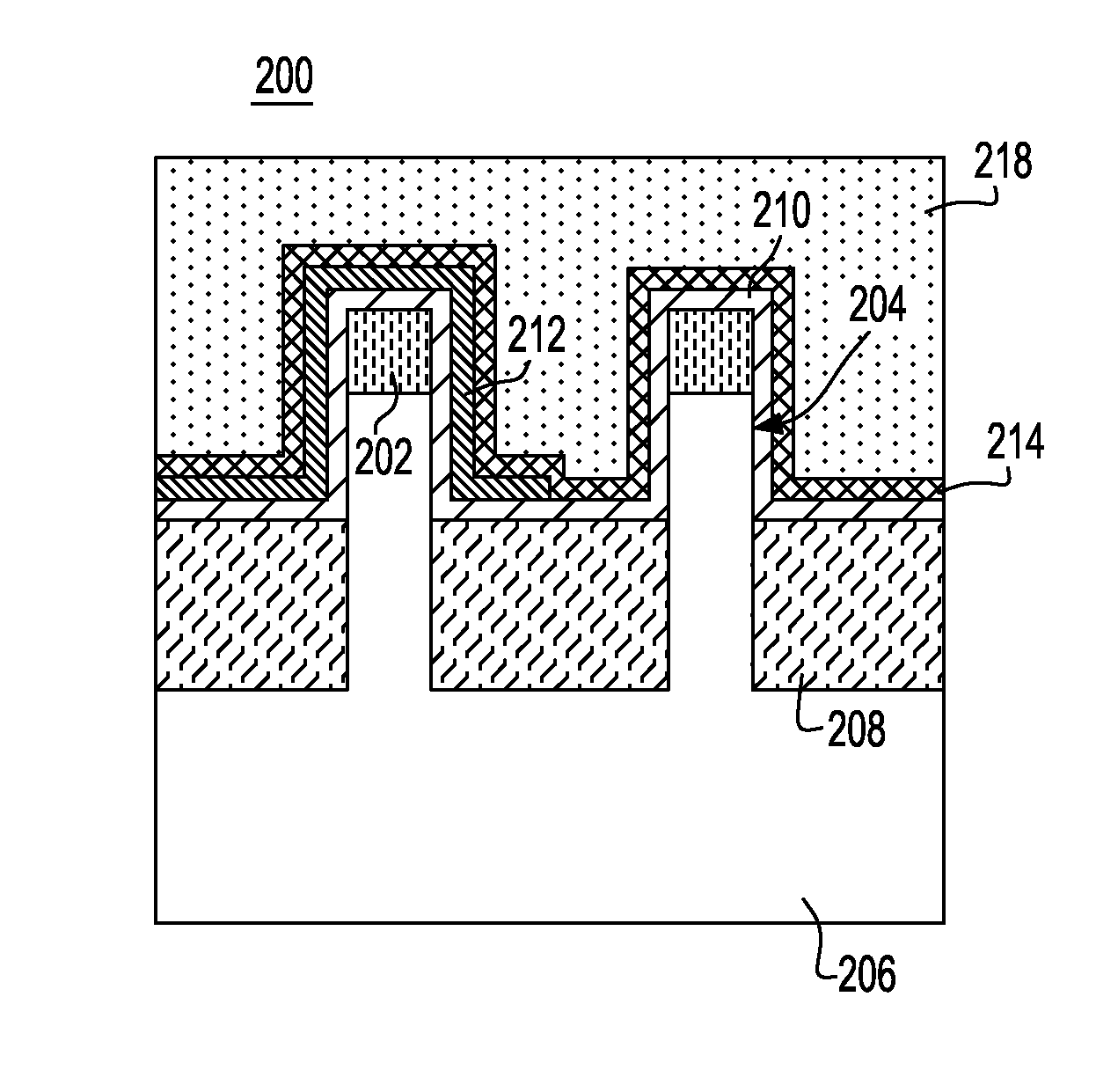
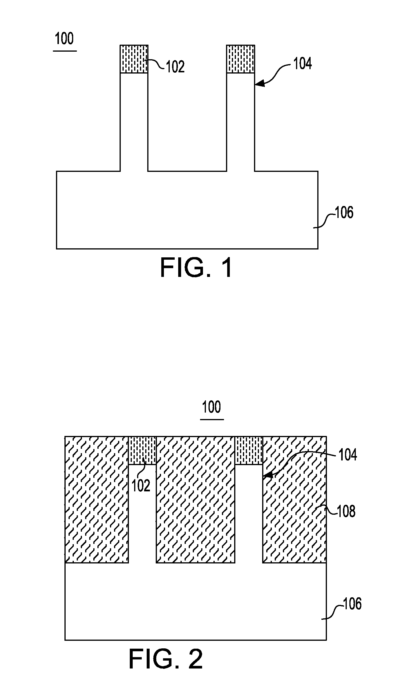
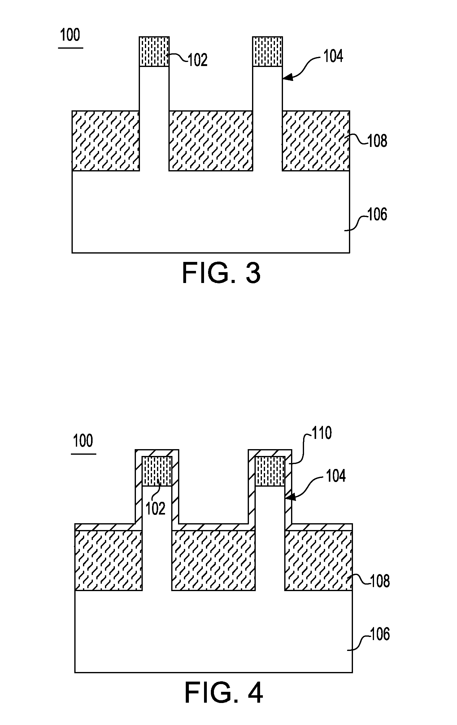
[0030]It will be appreciated that for simplicity and clarity of illustration, elements shown in the drawings are not necessarily drawn to scale. For example, the dimensions of some of the elements may be exaggerated relative to other elements for clarity. As previously stated, the present disclosure relates to a semiconductor structure including locally thinned semiconductor fins, and a method for manufacturing the same. Aspects of the present disclosure will now be described in detail with accompanying figures. It is noted that like reference numerals refer to like elements across different embodiments. As used herein, ordinals such as “first” and “second” are employed merely to distinguish similar elements, and different ordinals may be employed to designate a same element in the specification and / or claims.

[0031]In a first exemplary semiconductor structure according to a first embodiment of the present disclosure can be formed by providing a semiconductor substrate, which can be ...


PUM

PropertyMeasurementUnit
sizeaaaaaaaaaa
sizeaaaaaaaaaa
widthaaaaaaaaaa

Abstract

A FinFet formed by depositing a thin layer of polycrystalline silicon followed by depositing a stress containing material, including a high Ge percentage silicon germanium film and / or a high stress W film on top of a polycrystalline silicon film. Freeing space between fins allows stressor films to be deposited closer to the transistor channel, improving the proximity of the stress containing material to the transistor channel and enhancing the stress coupling efficiency by defining a ratio between stress level in the stressor film and stress transferred to the channel for a mobility enhancement. The stress level is enhanced by patterning by removing the n-type workfunction metal from the p-FinFET. After stripping off the soft or hard mask, the p-type workfunction metal is deposited in the n- and p-FinFET regions. The freed space specifically for p-FinFet between the fins achieves an even higher stressor coupling to further boost the carrier mobility.

Description

FIELD OF THE INVENTION[0001]The present invention relates to the fabrication of semiconductor devices, and more particularly, to the formation of a gate stack of an n-type FET and a p-type FET to enhance the strain level in the channel to generate carrier mobility and drive current performance benefits in multigates or trigates.BACKGROUND AND RELATED ART[0002]Current techniques of forming gate stack in the FinFET device structure starts with depositing high-k metal dielectric material such as HfO2, Al2O3, or La2O3 by ALD process. The process can be done either following the fin formation, referenced as the “gate first” scheme (also referenced as the metal inserted polysilicon), or it can be done after the formation of the source and drain in a process referred to as “gate last”, (also referenced as “replacement metal gate” (RMG) scheme). The gate first and gate last refer to whether a metal electrode is deposited before or after the high temperature activation anneals of the flow. I...

Claims


Application Information

Patent Timeline
Patent Type & Authority Applications(United States)
IPC IPC(8): H01L29/66H01L29/78H01L29/165
CPCH01L29/66795H01L29/7848H01L29/785H01L29/165H01L21/823821H01L21/845H01L29/7845H01L27/0924H01L29/7846
Inventor BASKER, VEERARAGHAVAN S.KERBER, PRANITAWANG, JUNLIYAMASHITA, TANKOYEH, CHUN-CHEN
Owner IBM CORP
Why Eureka
Try Eureka