

Plasma processing apparatus and filter unit
- Summary
- Abstract
- Description
- Claims
- Application Information
AI Technical Summary
Benefits of technology
Problems solved by technology
Method used
Image

Examples
second exemplary embodiment
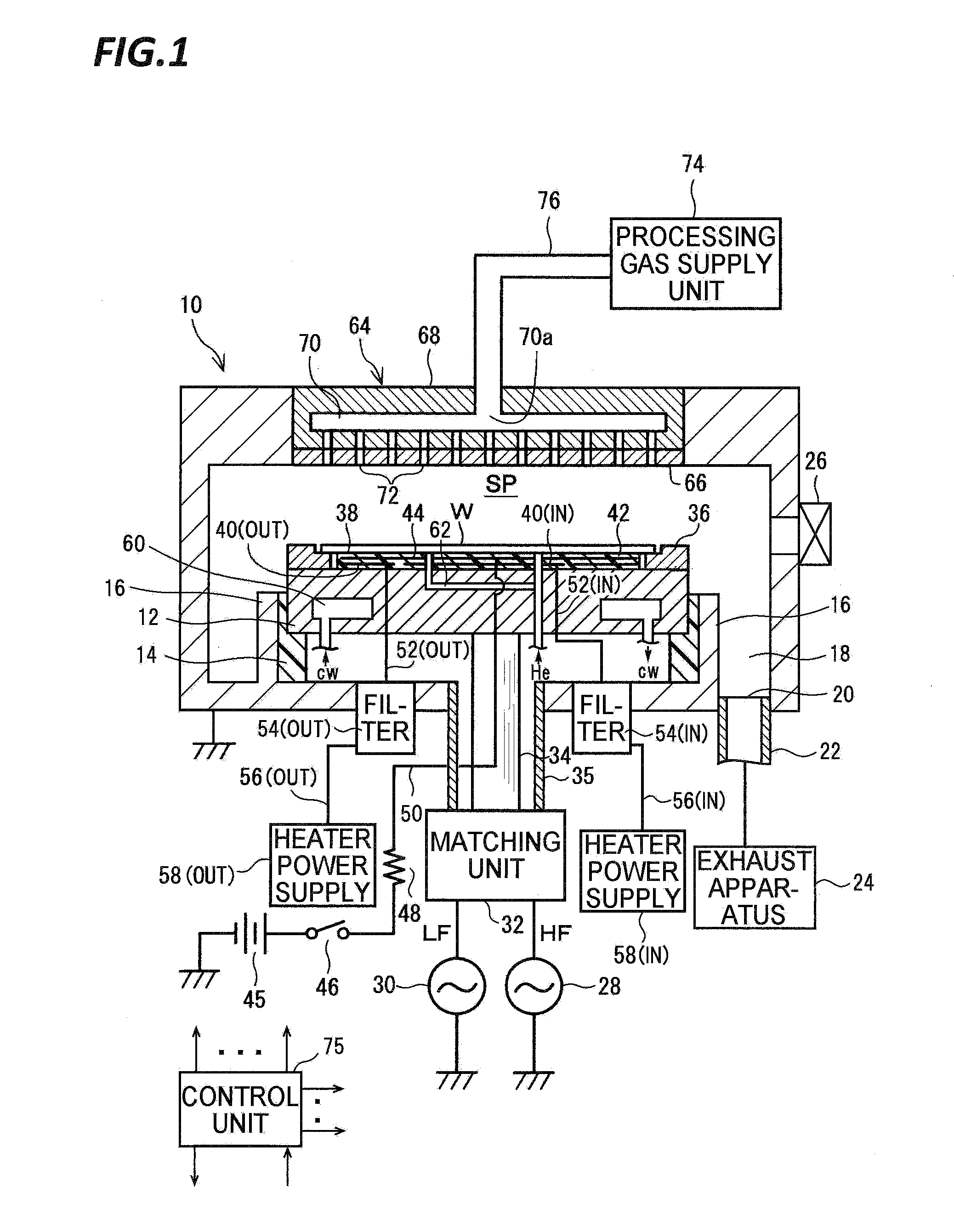
[0111]FIG. 10 illustrates a configuration of a plasma processing apparatus of a second exemplary embodiment. In the drawing, the components having the same configuration or function as those of the plasma processing apparatus of the first exemplary embodiment described above (FIG. 1) will be given the same symbols.
[0112]The plasma processing apparatus is configured as a capacitively coupled plasma etching apparatus of lower pat two-frequency / upper part one-frequency application type. This plasma etching apparatus has a main feature different from the plasma etching apparatus of the first exemplary embodiment described above (FIG. 1) in that a first high frequency wave HF for plasma generation is applied to an upper electrode 64, and second and third high frequency waves LF, MF having different frequencies are applied to the susceptor 12 in a superposed state so as to variously control the energy (bias) of ions drawn in a semiconductor wafer W in a more flexible manner. Here, the fre...
third exemplary embodiment
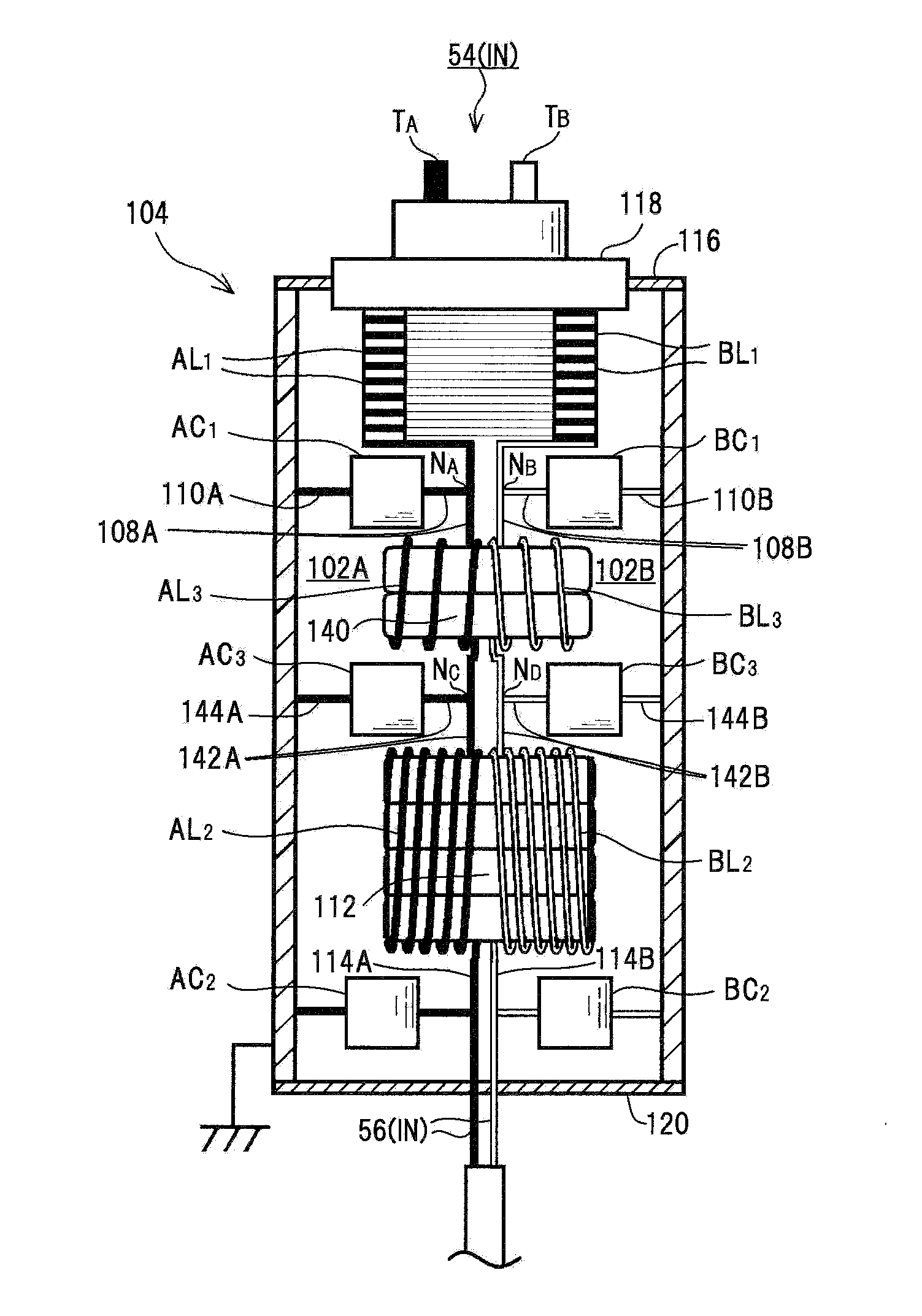
[0143]FIG. 14 illustrates a physical structure within a filter unit 54(IN) in a third exemplary embodiment. FIG. 15 illustrates an equivalent circuit of a filter 102A(102B) mounted in the filter unit 54(IN).
[0144]In the present exemplary embodiment, a fourth condenser AC4(BC4) electrically connected in parallel with the toroidal coil AL2(BL2) is disposed in the casing 104. The fourth condenser AC4(BC4) is a commercially available two-terminal type condenser and may be disposed laterally adjacent to the second condenser AC2(BC2) below the toroidal coil AL2(BL2), as illustrated in FIG. 14. One terminal of the condenser AC4(BC4) is connected to the upper terminal of the toroidal coil AL2(BL2) via a connection conductor 150A(150B), and the other terminal is connected to the lower terminal of the toroidal coil AL2(BL2) via the connection conductor 152A(152B).
[0145]In the present exemplary embodiment, as illustrated in FIG. 15, a second parallel resonance circuit 122 having a second paral...
modified example
Other Exemplary Embodiment or Modified Example
[0150]In the air core coil AL1(BL1), the ratio H / D of the coil diameter (outer diameter) D in relation to the coil length H may be set to be 1 or more. In general, as the air core coil AL1(BL1) is formed thin and long, H / D becomes large. To the contrary, as the air core coil AL1(BL1) is formed thick and short, H / D becomes small.
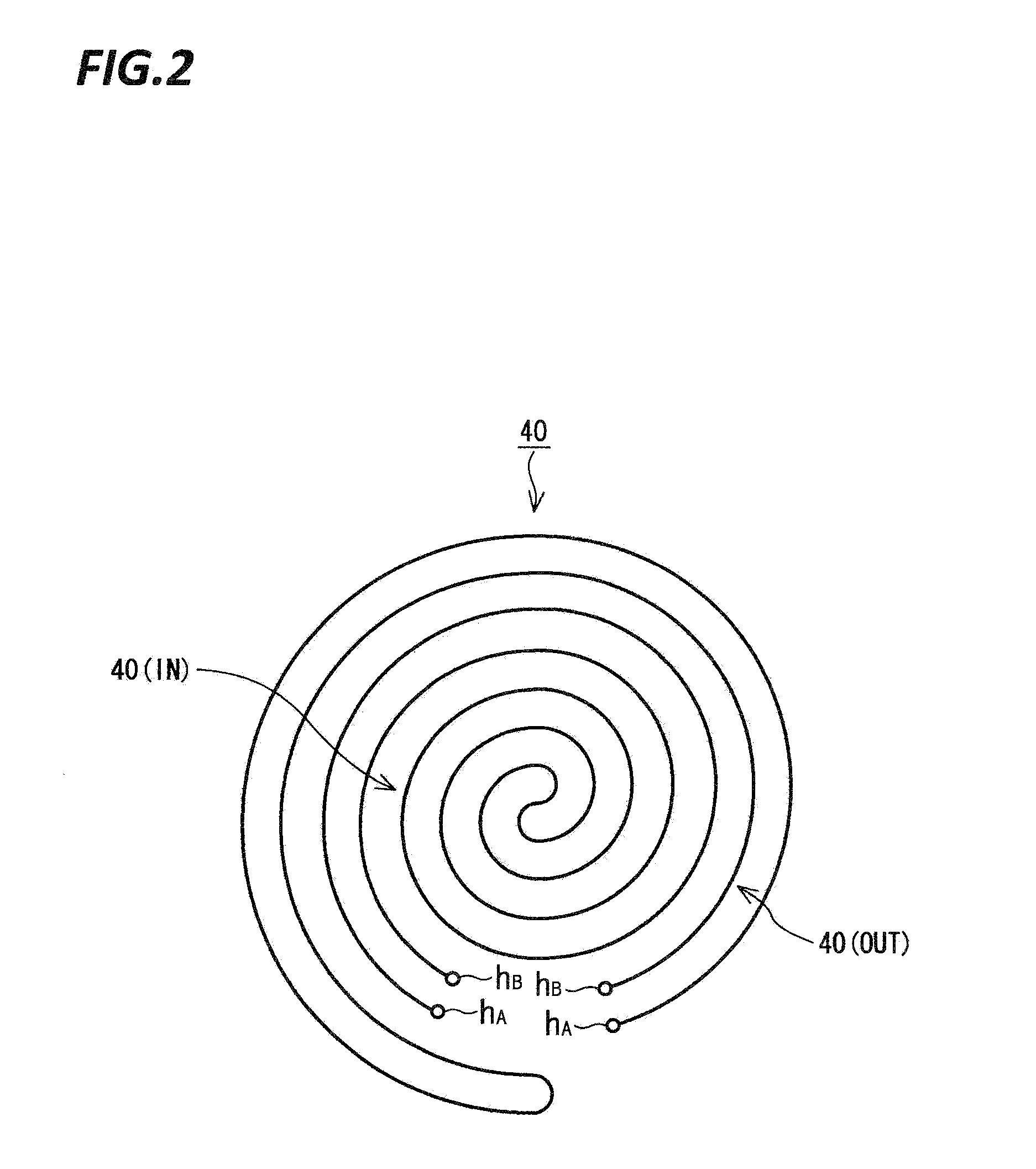
[0151]The toroidal coils AL2(BL2), AL3(BL3) in the exemplary embodiments described above are formed by winding coil conductors on single toroidal cores 112, 140 in which a plurality of single toroidal cores TC are stacked one on another. One toroidal coil or one set of toroidal coils may be also formed by connecting a plurality of toroidal coils of this type in series without holding a condenser therebetween.
[0152]In addition, as illustrated in FIG. 16, a composite toroidal coil AL may be used in which the composite toroidal coil AL is formed by connecting a plurality of single toroidal coils TR (three in the illu...
PUM
| Property | Measurement | Unit |
|---|---|---|
| Length | aaaaa | aaaaa |
| Thickness | aaaaa | aaaaa |
| Diameter | aaaaa | aaaaa |
Abstract
Description
Claims
Application Information