Semiconductor circuit board, semiconductor device using the same, and method for manufacturing semiconductor circuit board
- Summary
- Abstract
- Description
- Claims
- Application Information
AI Technical Summary
Benefits of technology
Problems solved by technology
Method used
Image

Examples
examples 1 to 10
Practical Examples 1 to 10 and Comparative Examples 1 to 3
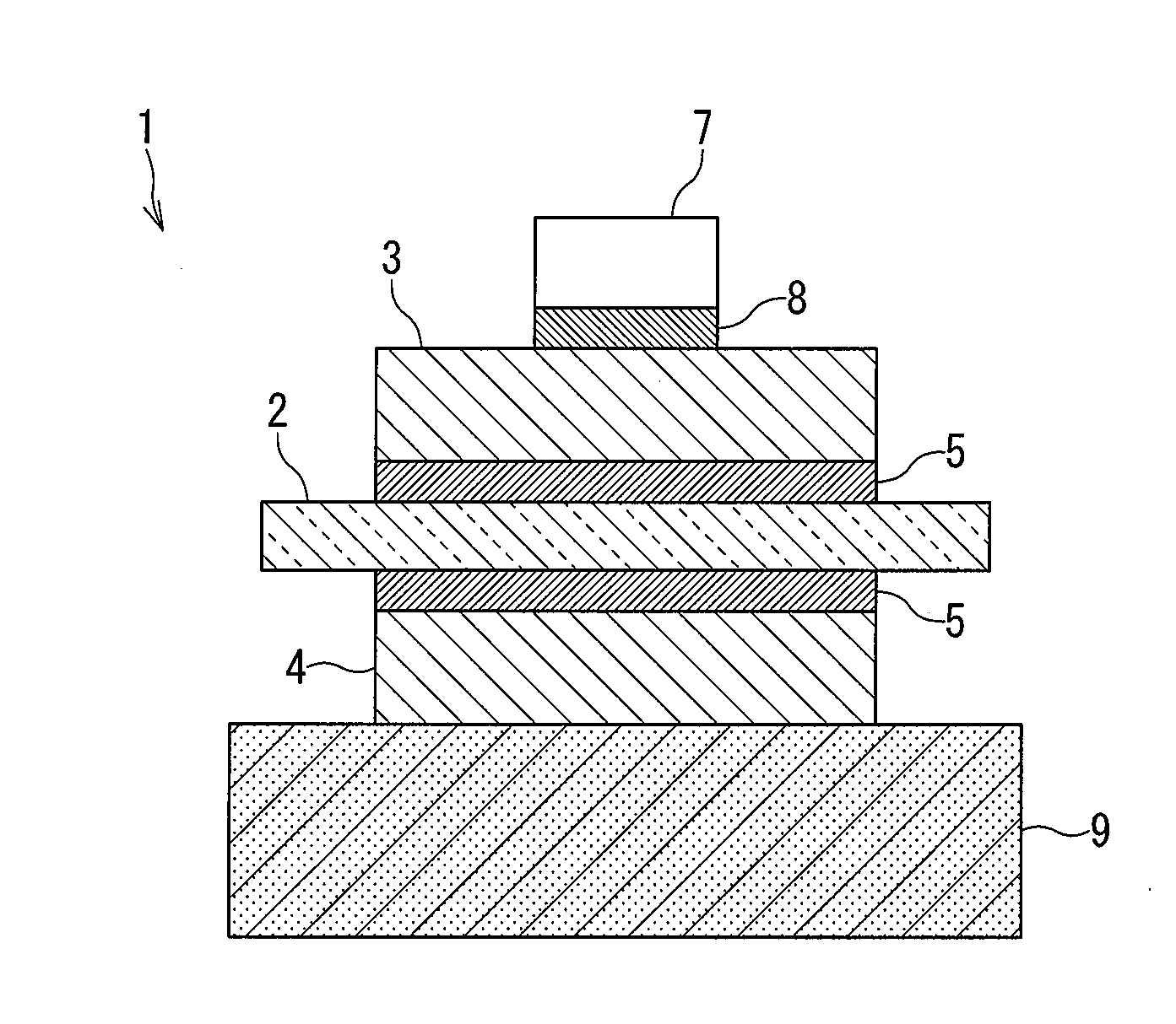
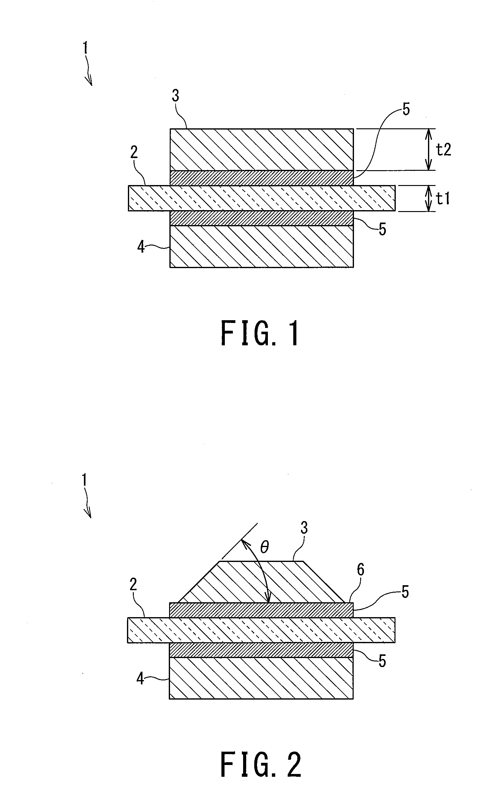
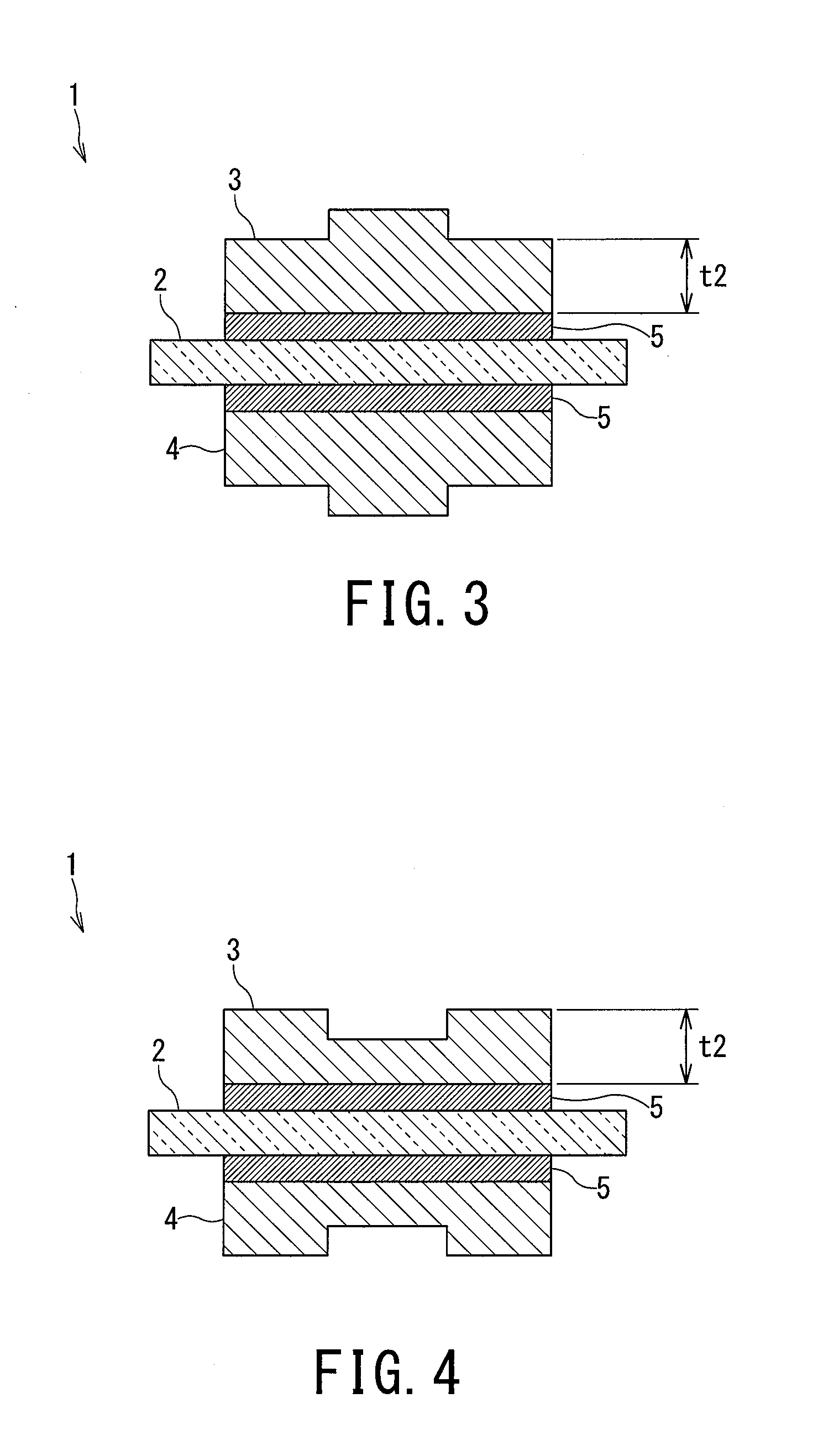
[0096]As insulating (ceramic) substrates (30 mm in length×35 mm in width), there were prepared alumina substrates (thickness: 0.635 mm, thermal conductivity: 15 W / m·K, three-point bending strength: 450 MPa), aluminum nitride substrates (thickness: 0.635 mm, thermal conductivity: 180 W / m·K, three-point bending strength: 400 MPa), and silicon nitride substrates (thickness: 0.320 mm, thermal conductivity: 90 W / m·K, three-point bending strength: 650 MPa).
[0097]Next, copper plates (25 mm in length×30 mm in width) were bonded to both sides of each insulating substrate by an active-metal brazing material method. Note that as the active-metal brazing material, a brazing material composed of 3 wt % of Ti, 30 wt % of Cu, and Ag for the rest was used, the brazing material was coated to a thickness of 15 μm, and the copper plates were heat-bonded at a temperature of 820 to 860° C. in a vacuum (10−3 Pa or lower). As the copper plates, oxy...
PUM
| Property | Measurement | Unit |
|---|---|---|
| Length | aaaaa | aaaaa |
| Length | aaaaa | aaaaa |
| Length | aaaaa | aaaaa |
Abstract
Description
Claims
Application Information
 - Generate Ideas
- Intellectual Property
- Life Sciences
- Materials
- Tech Scout
- Unparalleled Data Quality
- Higher Quality Content
- 60% Fewer Hallucinations
Browse by: Latest US Patents, China's latest patents, Technical Efficacy Thesaurus, Application Domain, Technology Topic, Popular Technical Reports.
© 2025 PatSnap. All rights reserved.Legal|Privacy policy|Modern Slavery Act Transparency Statement|Sitemap|About US| Contact US: help@patsnap.com