High electron mobility transistors with improved gates and reduced surface traps

a technology of electron mobility and transistors, applied in the direction of semiconductor devices, basic electric elements, electrical equipment, etc., can solve the problems of inability to switch or operate devices or transistors at too high frequency, inability to operate transistors at large voltages, and inability to meet the needs of applications, etc., to improve the adhesion of the gate, improve the effect of oxygenation and enhance device performan

Inactive Publication Date: 2015-09-17
QIU CHUNONG +4
View PDF8 Cites 15 Cited by
  • Summary
  • Abstract
  • Description
  • Claims
  • Application Information

AI Technical Summary

Benefits of technology

[0009]Present invention provides high mobility thin film transistors (HEMTs) with improved gates to enhance device performance. For those HEMTs, a first gate metal layer made of chromium alloy or tungsten alloy is deposited to minimize effects of oxygen and water trapped in the surface region of the Schottky barrier layer, to improve adhesion of the gate and increase stability and reliability of the thin film transistors.

Problems solved by technology

For electrical signals at frequencies higher than 1 GHz, the silicon based devices may not be suitable for applications such as microwave and millimetre wave switching and amplification because of the relatively low charge carrier mobility and breakdown electric field of the doped silicon.
Due to the relatively low charge carrier mobility of in the order of 1,000 cm2 / V-sec, the devices or transistors can not be switched or operated at too high a frequency.
Due to the relatively low breakdown electric field of about 0.3×10⁶ V / cm, the transistors can not be operated at large voltages and hence at high power because of small dimensions / thicknesses and easy material breakdown.
One of the issues of the III-nitride HEMTs is the stability and integrity of the gate for the controlling of channel charges especially for high power switching and amplification.
There is often an unwanted effect due to a difference in expansion coefficients between the gate material, which is a metal, and the channel layers, which are composite III-nitride films, InGaN, AlGaN and GaN in this case.
Therefore, during device fabrication and subsequent operation, there are substantial strain and / or stresses in the composite channel layers of InGaN, AlGaN and GaN.
These strain or stresses can lead to degradation of the gate hence the HEMT it attaches to.
When the HEMT is operated in ON state at a high power level, significant amount of unwanted heat will be dissipated into the channel region, leading to a temperature rise of the channel layers and adjacent transistor components including the drain contact, the source contact and more importantly the gate.
Due to the difference in thermal expansion coefficient between the semiconductor channel layers and the gate materials, significant strain or stresses can be induced in the gate and in the channel.
Under more severe situation, even a partial microscopic deformation of the gate or a partial detachment of the gate from the channel layers may take place, leading to degradation of the gate.
Such degradation may lead to incomplete or non-continuous contact between the gate and the channel layers which will reduce the modulation effect of the channel and the stability of the gate.
These oxygen and water molecules may not be removed completely prior to the deposition of the gate metal layers and will get trapped between surface of the Schottky barrier layer in the channel region and the gate.
If left alone, those trapped oxygen and water molecules will increase the interface states and result in a HEMT with unwanted non-constant drain current output characteristics.

Method used


Image

  • High electron mobility transistors with improved gates and reduced surface traps
  • High electron mobility transistors with improved gates and reduced surface traps
  • High electron mobility transistors with improved gates and reduced surface traps

Examples


Embodiment Construction

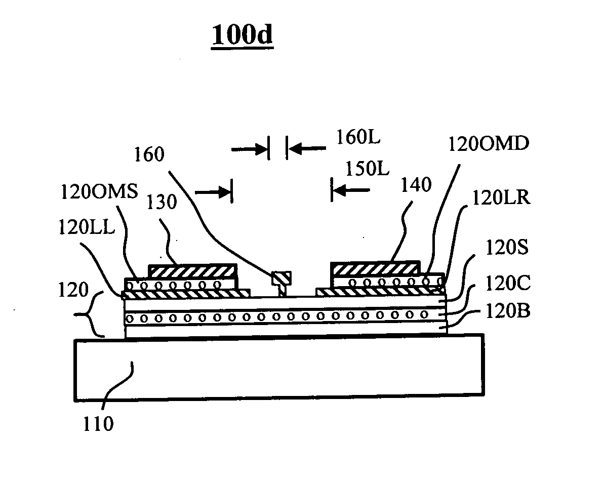
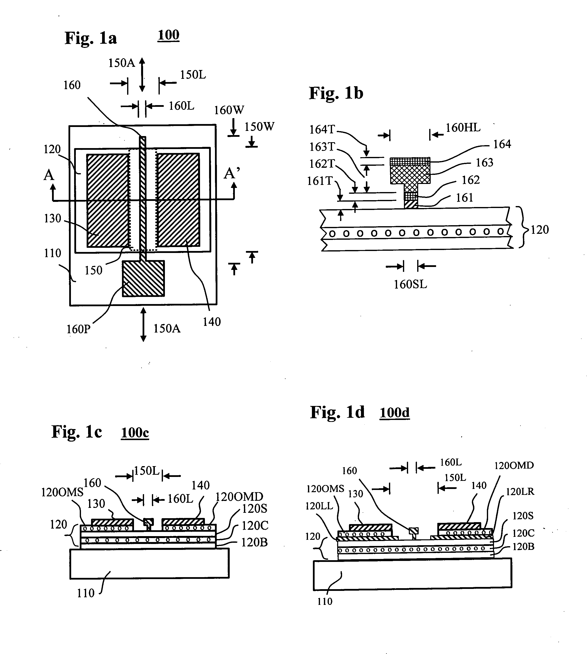
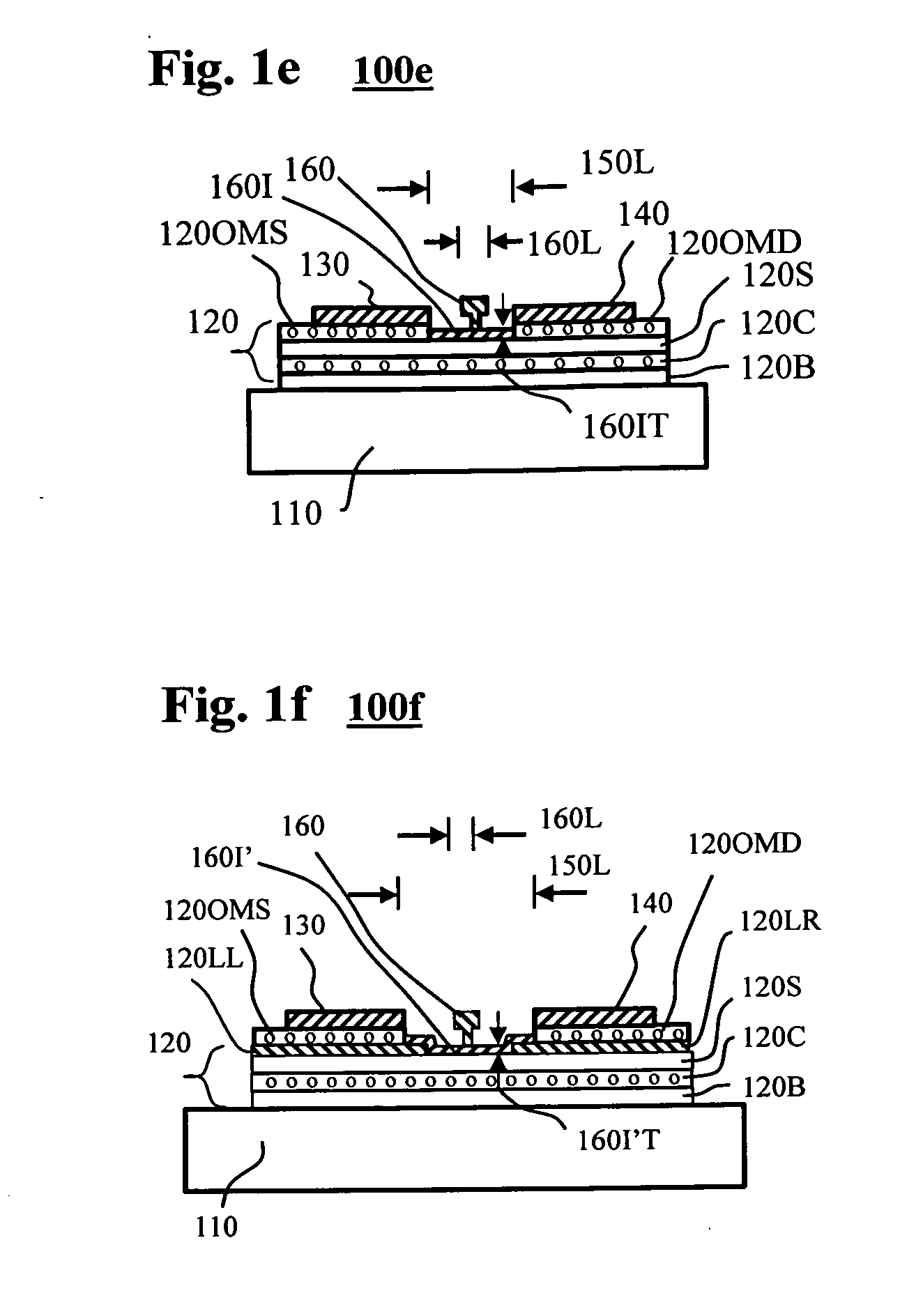
[0014]According to one embodiment of this invention, as shown in FIG. 1a, a high electron mobility transistor (HEMT, 100) with improved gate performance for power switching or for millimetre wave circuit applications comprises a substrate (110); a composite epitaxial channel layers (120); a source contact (130) and a drain contact (140) defining a channel region (150) having a channel region long axis (150A), a channel region width (150W) and a channel region length (150L); and a gate (160) having a gate length (160L), a gate width (160W) and a gate pad (160P). The gate (160) makes a rectifying or Schottky contact to the channel region (150). Resistance between the drain (140) and the source (130) is regulated by a voltage applied between the gate (160) and the source (130).

[0015]The gate (160) comprises a plurality of layers with a first gate layer (161, see FIG. 1b) having a first gate layer thickness (161T), a second gate layer (162) with a second gate layer thickness (162T) for ...


PUM

PropertyMeasurementUnit
heightaaaaaaaaaa
heightaaaaaaaaaa
heightaaaaaaaaaa

Abstract

The present invention is related to high electron mobility transistors for power switching and microwave amplification and switching. More specifically, it related to a high electron mobility transistor with an improved gate to enhance the performance. When fabricating a high electron mobility thin film transistors, a first gate metal layer made of chromium alloy or tungsten alloy is deposited to reduce surface traps and to enhance the stability and integrity of the gates.

Description

FIELD OF INVENTION[0001]Present invention is related to high electron mobility transistors for power switching and microwave amplification and switching. More specifically, it related to a high electron mobility transistor with an improved gate to reduce surface traps and to enhance the stability and the performance of the devices.BACKGROUND OF THE INVENTION[0002]For electronic switching and amplification of electrical signals at low frequencies of about or below 1 GHz, silicon based devices in metal-oxide-semiconductor (MOS) structure or bipolar junction transistor (BJT) structure are often used. Silicon devices for such applications include MOS field effect transistors (MOSFET), insulated gate bipolar transistors (IGBT) and lightly doped drain MOS field effect transistors (LDMOSFET). For electrical signals at frequencies higher than 1 GHz, the silicon based devices may not be suitable for applications such as microwave and millimetre wave switching and amplification because of the...

Claims


Application Information

Patent Timeline
Patent Type & Authority Applications(United States)
IPC IPC(8): H01L29/423H01L29/778
CPCH01L29/778H01L29/42372H01L21/28581H01L21/28587H01L29/2003H01L29/42316H01L29/42376H01L29/475H01L29/7783
Inventor QIU, CHUNONGWU, JAY-HSINGQIU, CINDY X.SHIH, YI-CHISHIH, ISHIANG
Owner QIU CHUNONG
Why Eureka
Try Eureka