Solar cell and method of manufacturing therefor

a technology of solar cells and manufacturing methods, applied in the field of solar cells, can solve the problems of increasing the processing cost of fabricating nanostructures and reducing economic efficiency, and achieve the effects of increasing photoelectric conversion efficiency, and improving photoelectric conversion efficiency

Active Publication Date: 2015-10-08
JUN YOUNG KWON
View PDF8 Cites 13 Cited by
  • Summary
  • Abstract
  • Description
  • Claims
  • Application Information

AI Technical Summary

Benefits of technology

[0052]In a solar cell according to the present invention, since an electrical polarization layer, in which a built-in electric field is formed by spontaneous polarization or remnant polarization, is disposed adjacent to a light-absorbing layer of the solar cell, the recombination of electrons and holes, which are generated in a p-n junction semiconductor due to optical absorption, may be reduced and collection efficiency of an electrode may be simultaneously improved through the built-in electric field to increase photoelectric conversion efficiency.
[0053]Also, with respect to a CIGS thin film solar cell according to an aspect of the present invention, in a case where an electrical polarization layer is formed by replacing a typic...

Problems solved by technology

However, since a technique disclosed in the following Patent Document 1 additionally requires energy and equipment to generate the mechanical vibration, economic efficiency may be reduced.
Howev...

Method used


Image

  • Solar cell and method of manufacturing therefor
  • Solar cell and method of manufacturing therefor
  • Solar cell and method of manufacturing therefor

Examples


example 1

[0100]In Example 1 of the present invention, a CIGS thin film solar cell was manufactured by the following process.

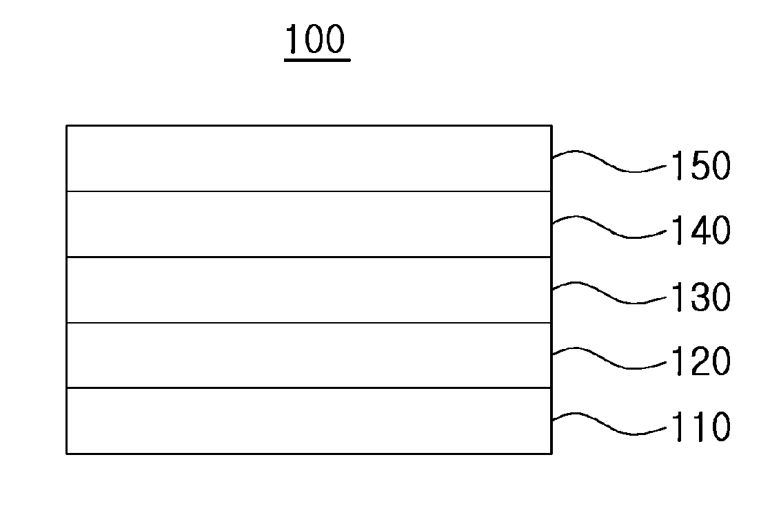
[0101]First, a lower electrode was formed by depositing a molybdenum (Mo) layer on a SLG substrate to a thickness of about 1 μm using a sputtering method. Subsequently, a CIGS thin film was deposited to a thickness of about 2 μm to form a light-absorbing layer.

[0102]As a method of forming the CIGS light-absorbing layer, there are a co-evaporation method in which deposition is performed by individually and simultaneously evaporating elements, such as Cu, indium (In), gallium (Ga), and selenium (Se), in a high vacuum atmosphere and heating the substrate in a temperature range of 500° C. to 600° C., and a two-stage method in which a precursor including elements, such as Cu, Ga, and In, or a precursor including Cu, Ga, In, and Se is used to form a thin film, and selenization is then performed in a H2Se gas or Se vapor atmosphere.

[0103]Also, as a method of forming the precur...

example 2

[0139]Although the solar cell was manufactured by using a vacuum deposition method in Example 1 of the present invention, but a solar cell may be formed by using a non-vacuum deposition method such as chemical bath deposition (CBD), spin coating, doctor-blade coating, drop-casting, screen printing, and inkjet printing, and a solar cell according to Example 2 of the present invention may include an electrical polarization layer which was formed by a wet coating method.

[0140]First, a lower electrode was formed on a SLG substrate by coating the substrate with an Ag or Cu layer to a thickness of about 1 μm using a spin coating method. Subsequently, in order to manufacture CIGS formed of a semiconductor having a p-n junction structure, a precursor solution including constituent elements, such as Cu, In, Ga, Se, and sulfur (S), was prepared, and a light-absorbing layer was formed to a thickness of about 3 μm by coating the substrate with the precursor solution by spin coating or doctor-bl...

example 3

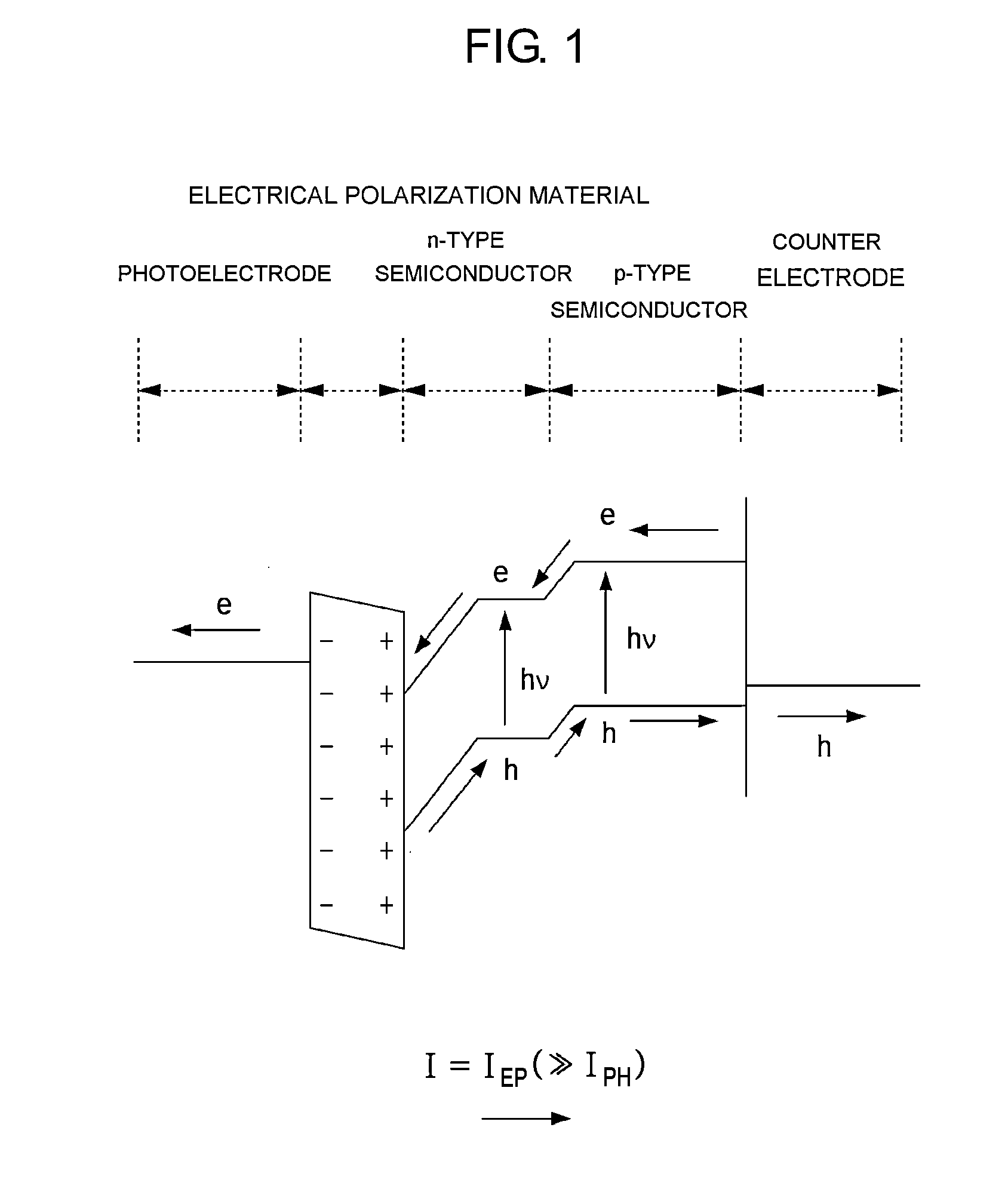
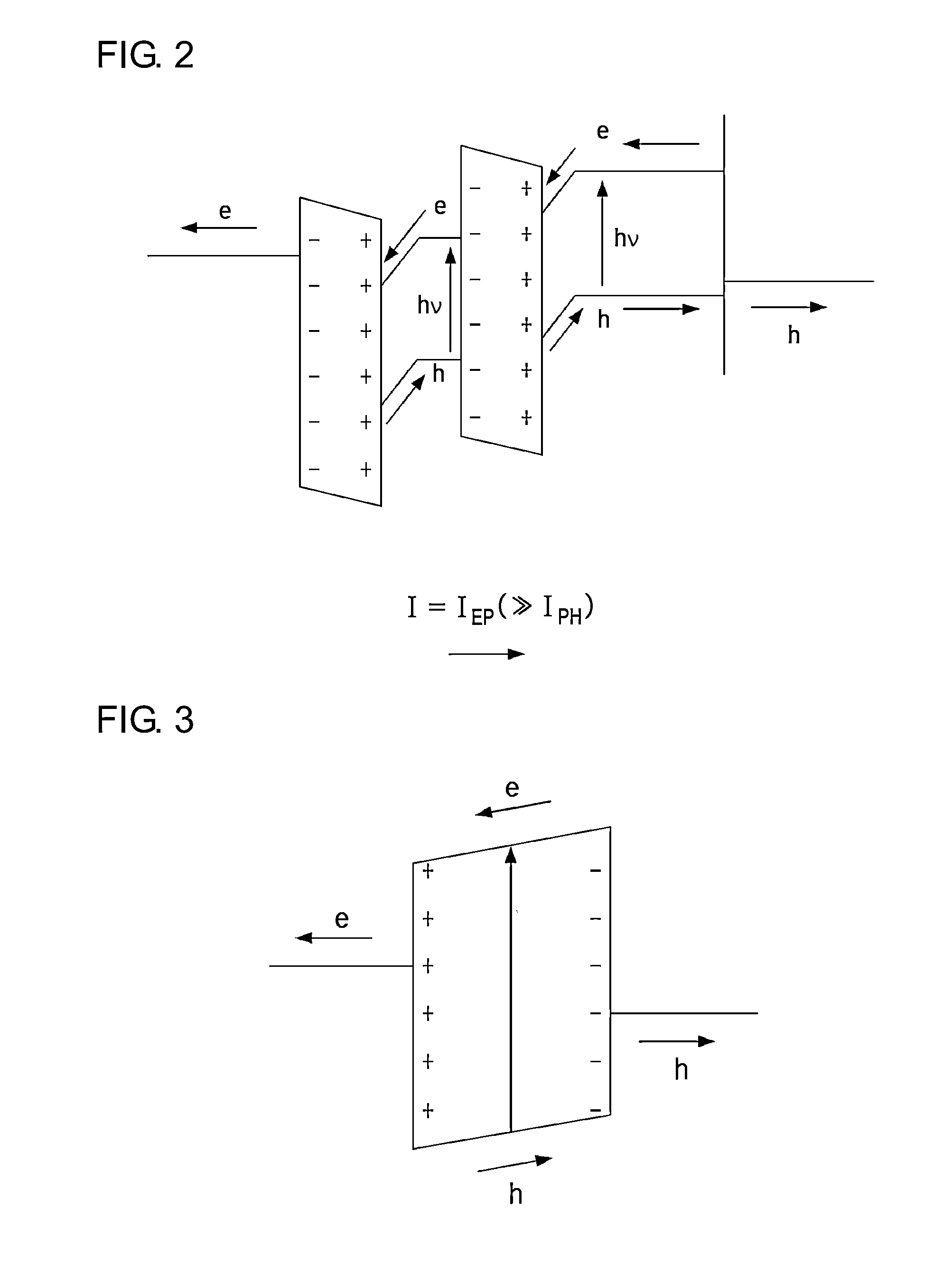
[0145]In Examples 1 and 2 of the present invention, the case of forming an electrical polarization layer in a solar cell was described as an example, but an electrical polarization layer may be connected to the outside of the solar cell in series. That is, in a typical solar cell structure composed of substrate-lower electrode-light-absorbing layer (or p-n junction semiconductor layer)-upper electrode, when an electrical polarization layer is formed between the substrate and the lower electrode, above the upper electrode, or at both sides thereof so as to be connected to the electrode in series, an effect of applying a forward electric field to electrons and holes, which are collected in a solar cell, may be obtained by using spontaneous polarization of the electrical polarization layer or using remnant polarization which is formed by applying an electric field to the electrical polarization layer.

[0146]Even in this case, the above-described method of forming an electrical polarizat...


PUM


Abstract

The present invention relates to a structure of a solar cell for improving photoelectric conversion efficiency of the solar cell, and a manufacturing method therefor. One aspect of the solar cell according to the present invention relates to a solar cell having a light-absorbing layer formed between two electrodes arranged to face each other, wherein an electrical polarization layer comprising an electrical polarization material forming an inner electrical field is formed between the electrodes and the light-absorbing layer.

Description

TECHNICAL FIELD[0001]The present invention relates to a solar cell and a method of manufacturing the same, and more particularly, to a structure of a solar cell, in which photoelectric conversion efficiency of the solar cell is improved by disposing an electrical polarization layer, which forms a built-in electric field due to spontaneous polarization and / or remnant polarization characteristics, adjacent to a light-absorbing layer in a crystalline silicon solar cell as well as a thin film solar cell such as a Cu(In,Ga)Se2 (CIGS) solar cell and a dye-sensitized solar cell, and a method of manufacturing the same.BACKGROUND ART[0002]A thin film solar cell technique is an advanced solar cell technique that is compared to a technique of crystalline silicon (Si) solar cell which currently has the largest market share, wherein the thin film solar cell has a higher efficiency than the crystalline Si solar cell and may be manufactured at a lower cost.[0003]Various types of thin film solar ce...

Claims


Application Information

Patent Timeline
IPC IPC(8): H01L31/0224H01L31/075H01L31/18
CPCH01L31/022425H01L31/075H01L31/18Y02E10/541H01L31/06H01L31/0749Y02E10/548Y02P70/50H01L31/0322H01L31/0326
Inventor JUN, YOUNG KWON
Owner JUN YOUNG KWON
Why Eureka
Try Eureka