Diffractive optical elements and methods for patterning thin film electrochemical devices

a thin film electrochemical and diffractive optical element technology, applied in sustainable manufacturing/processing, batteries, instruments, etc., can solve the problems of limiting the utilization of substrate area, complex and costly process, and still need to overcome, so as to eliminate some complexities and costs of use, the effect of low cost and high throughpu

Inactive Publication Date: 2015-10-15
APPLIED MATERIALS INC
View PDF19 Cites 3 Cited by
  • Summary
  • Abstract
  • Description
  • Claims
  • Application Information

AI Technical Summary

Benefits of technology

[0005]In general, the invention relates to mask-less laser direct patterning of thin film electrochemical devices, such as thin film batteries (TFBs) and electrochromic (EC) devices, and more specifically to the application of diffractive optical elements for laser patterning of thin film electrochemical devices. The present invention may include laser direct patterning with the use of diffractive optical elements for, among others: die patterning of thin film electrochemical devices after all active layers have been deposited; selective ablation of cathode / anode material from corresponding current collectors; selective ablation of electrolyte material from current collectors; and selective ablation of protective coating material from current collectors, including permeation protection coatings. Diffractive optical elements may be combined with traditional laser scribing equipment for the laser patterning according to the present invention. Many different thin film electrochemical device integration schemes can be developed based on diffractive optical elements according to the present invention, some of the schemes enabling the high throughput and low cost desired in volume production of electrochemical devices. For example, the present invention allows all blanket deposition of device layers, followed by laser device patterning with a diffractive optical element, eliminating some of the complexities and costs of using shadow masks and eliminating some of the issues and limitations associated with small Gaussian beam based direct patterning.

Problems solved by technology

However, there are challenges that still need to be overcome to allow cost effect high volume manufacturing of TFBs.
One of the most critical challenges pertains to the current state-of-the-art device patterning technology wherein various physical shadow masks are used during deposition of the device layers, Using shadow masks results in a complex and costly process as influenced by the following disadvantages: (1) a significant capital investment is required to handle (including precision alignment) and clean the masks, especially for large area substrates; (2) the use of shadow masks limits utilization of the substrate area (due to poor alignment capability and stability of alignment during processing) and affects product yield (due primarily to particulate generation); and (3) places constraints on the process (specifically, process limited to low power and low temperature) caused by potential thermal expansion induced alignment issues.
However, these processes also have their challenges.
For example, the lithography brings in new materials in the photo-resists and associated dry or wet etch and clean chemicals and processes, which can lead to potentially adverse materials interactions at various interfaces, leading to compromise in device functionalities and performances, not to mention significant additional costs.
Laser scribing / patterning technology, while it avoids the complexities of the lithography processes and provides significant scalability and cost advantages over both lithography and physical mask based patterning, needs precise galvanometer scanners and the typical Gaussian profile of the laser beam is not well suited for ablating relatively large areas (relative to the beam cross-section), which will add cost to the equipment and process.

Method used


Image

  • Diffractive optical elements and methods for patterning thin film electrochemical devices
  • Diffractive optical elements and methods for patterning thin film electrochemical devices
  • Diffractive optical elements and methods for patterning thin film electrochemical devices

Examples


Embodiment Construction

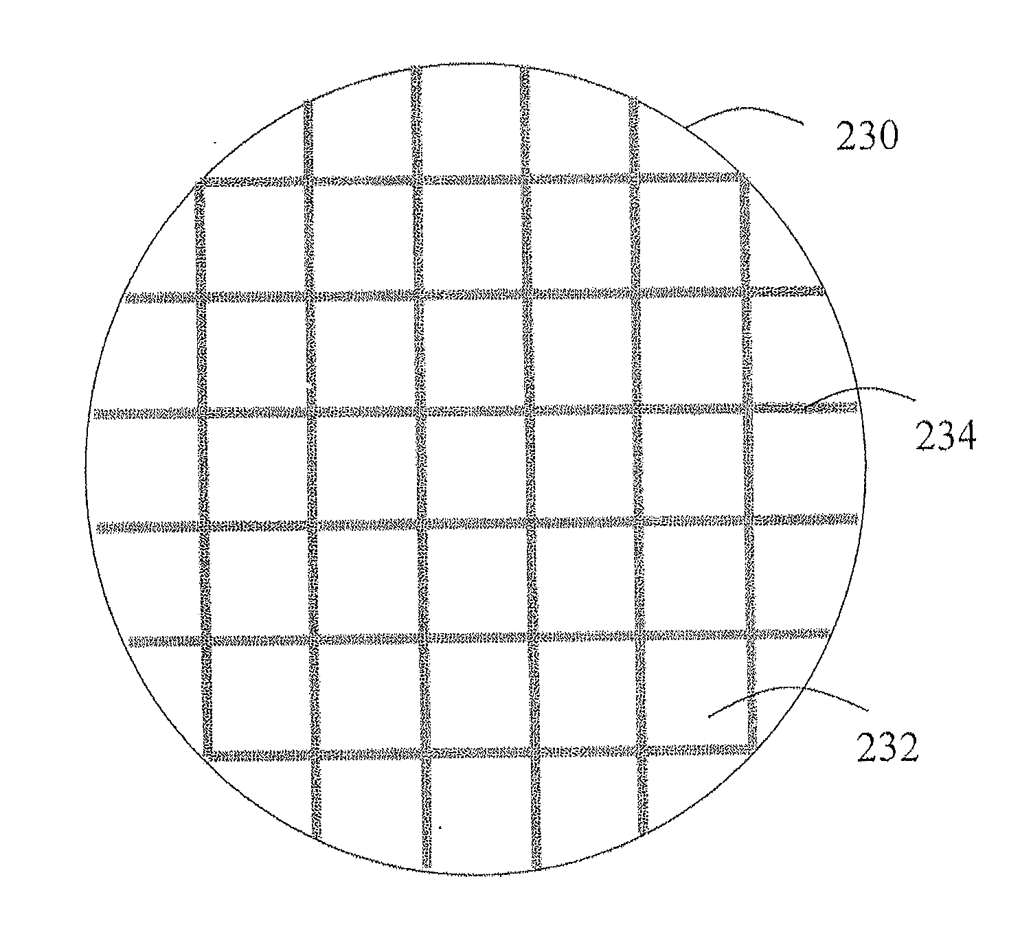
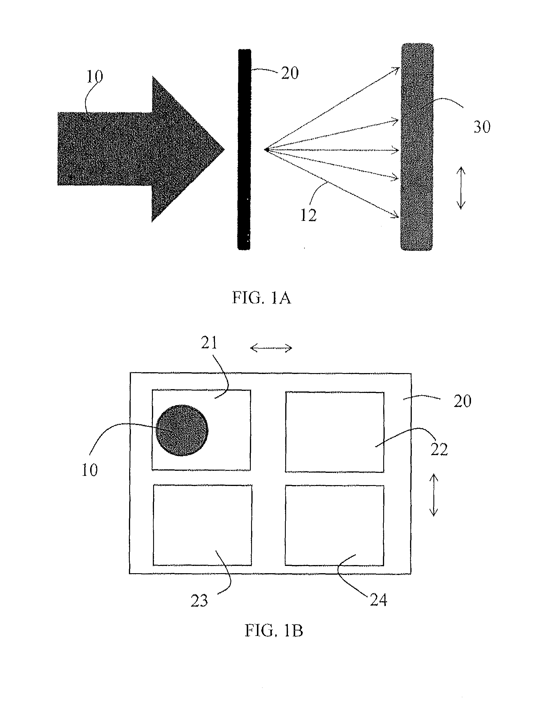
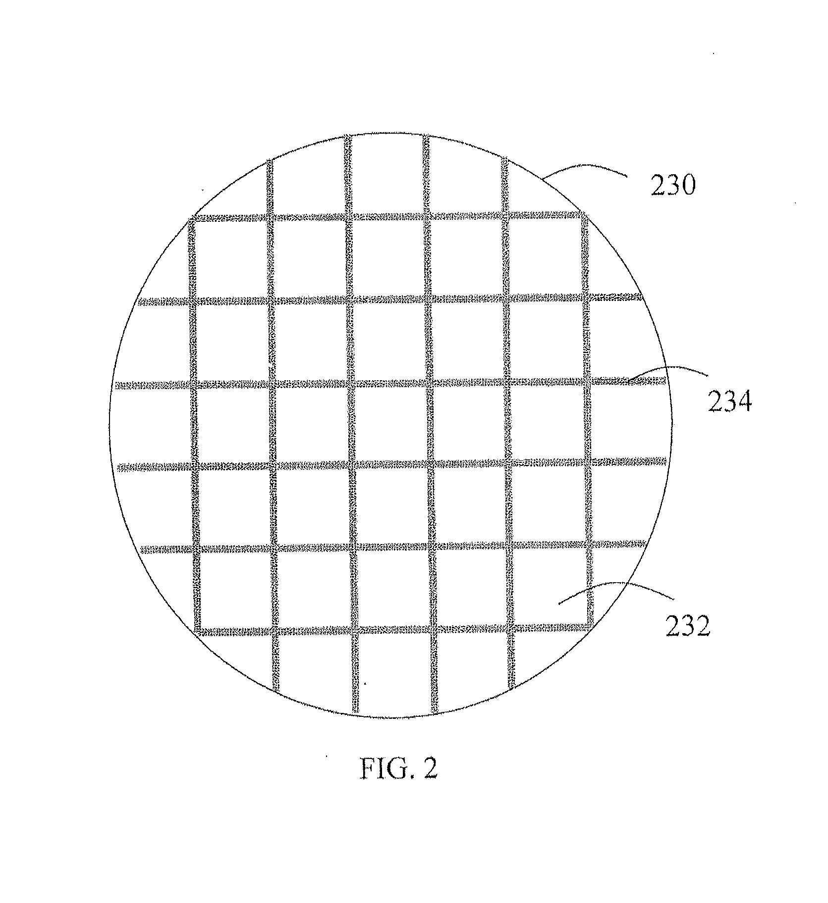
[0024]Embodiments of the present invention will now be described in detail with reference to the drawings, which are provided as illustrative examples of the invention so as to enable those skilled in the art to practice the invention. Notably, the figures and examples below are not meant to limit the scope of the present invention to a single embodiment, but other embodiments are possible by way of interchange of some or all of the described or illustrated elements. Moreover, where certain elements of the present invention can be partially or fully implemented using known components, only those portions of such known components that are necessary for an understanding of the present invention will be described, and detailed descriptions of other portions of such known components will be omitted so as not to obscure the invention. In the present specification, an embodiment showing a singular component should not be considered limiting; rather, the invention is intended to encompass ...


PUM

PropertyMeasurementUnit
wavelengthsaaaaaaaaaa

Abstract

A method of fabricating an electrochemical device, comprising: depositing device layers, including electrodes and corresponding current collectors, and an electrolyte layer, on a substrate; and directly patterning at least one of said device layers by a laser light pattern generated by a laser beam incident on a diffractive optical element, the laser light pattern directly patterning at least an entire device in a single laser shot. The laser direct patterning may include, among others: die patterning of thin film electrochemical devices after all active layers have been deposited; selective ablation of cathode/anode material from corresponding current collectors; and selective ablation of electrolyte material from current collectors, Furthermore, directly patterning of the electrochemical device may be by a shaped beam generated by a laser beam incident on a diffractive optical element, and the shaped beam may be moved across the working surface of the device.

Description

CROSS-REFERENCE TO RELATED APPLICATIONS[0001]This application claims the benefit of U.S. Provisional Application No. 61 / 718,656 filed Oct. 25, 2012.FIELD OF THE INVENTION[0002]Embodiments of the present invention relate to laser light patterning thin film electrochemical devices, such as thin film batteries and electrochromic devices, using diffractive optical elements and in further embodiments shaped-beams.BACKGROUND OF THE INVENTION[0003]Thin film batteries (TFB), with their unsurpassed properties, have been projected to dominate the micro-energy application space. However, there are challenges that still need to be overcome to allow cost effect high volume manufacturing of TFBs. One of the most critical challenges pertains to the current state-of-the-art device patterning technology wherein various physical shadow masks are used during deposition of the device layers, Using shadow masks results in a complex and costly process as influenced by the following disadvantages: (1) a s...

Claims


Application Information

Patent Timeline
Patent Type & Authority Applications(United States)
IPC IPC(8): G02B27/42B23K26/36G02F1/153
CPCG02B27/4233B23K26/365G02F1/153H01M4/0402H01M2010/0495H01M2220/30B23K26/361Y02E60/10Y02P70/50
Inventor SONG, DAOYINGKWAK, LEO B.ADAMS, BRUCE E.MOFFITT, THEODORE P.
Owner APPLIED MATERIALS INC
Why Eureka
Try Eureka