Photodiode array having a charge-absorbing doped region

a photodiode array and charge-absorbing technology, applied in the field of photodiode arrays, can solve the problems of unable to obtain good dark area rendering, limited output signal by the maximum integration capacity of the detector, and all the more problems

Active Publication Date: 2015-12-24
NEW IMAGING TECH
View PDF3 Cites 6 Cited by
  • Summary
  • Abstract
  • Description
  • Claims
  • Application Information

AI Technical Summary

Problems solved by technology

However, the output signal is limited by the maximum integration capacity of the detector.
For scenes having high contrast, it is often impossible to obtain good rendering of dark areas and at the same time to maintain the bright areas saturation-free.
This is all the more problematic for night vision for which a sensor array with InGaAs photodiodes is often intended.
Another problem with this approach is the fact that the steps of etching and photodiode anode diffusion are two separate steps in the manufacturing process requiring different masks.
Mask alignment errors can create additional non-uniformities between the photodiodes of an array.

Method used


Image

  • Photodiode array having a charge-absorbing doped region
  • Photodiode array having a charge-absorbing doped region
  • Photodiode array having a charge-absorbing doped region

Examples


Embodiment Construction

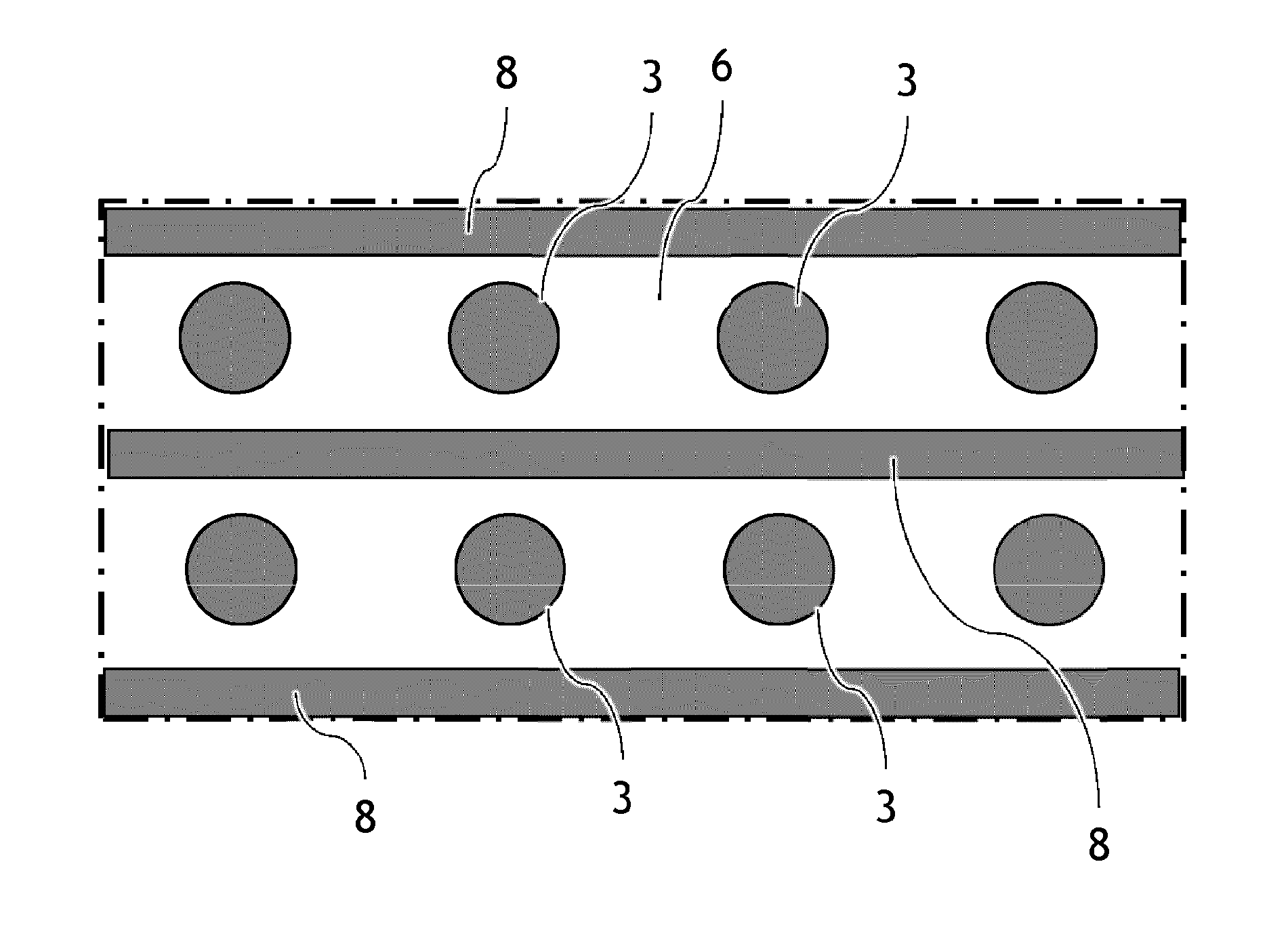
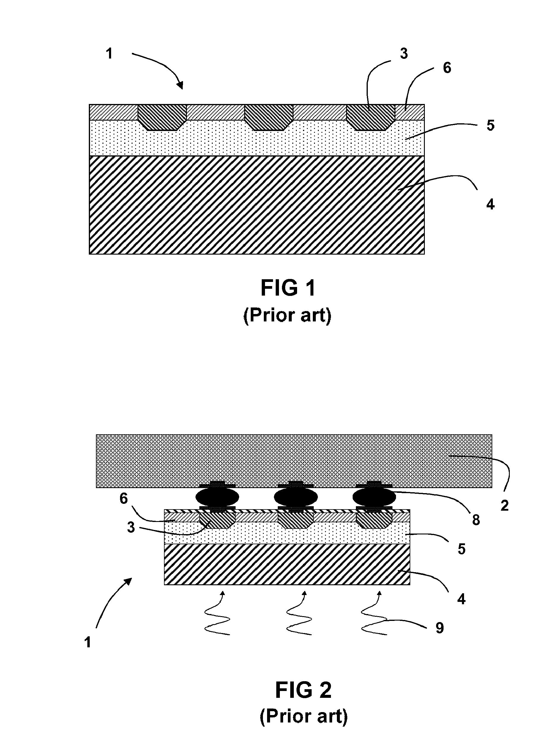
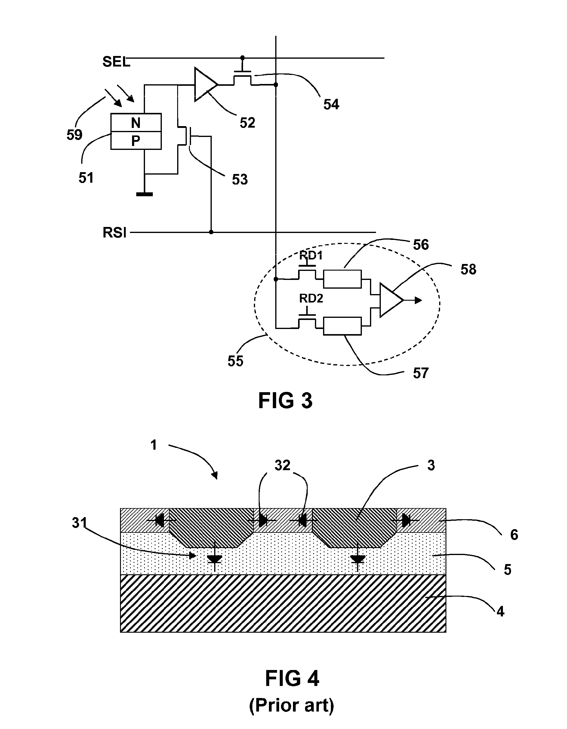
[0054]In a prior art structure as illustrated in FIG. 1, it can be ascertained that each photodiode contains several PN junctions one of which is desired and a certain number of which are parasitic. These PN junctions are illustrated in FIG. 4. The PN junctions 31 between the anodes 3 and the active layer 5 are desired and form the diodes of the photodiode array.

[0055]The parasitic lateral PN junctions 32, between the anodes 3 and the passivation layer 6, form a possible electrical pathway between neighbouring photodiodes via the passivation layer.

[0056]A conventional read-out circuit, in a capacitor, integrates the reverse current in the photodiode by applying a reverse bias thereto. In this configuration, the parasitic lateral junctions 32 in the photodiodes are reverse biased at the same time, having the effect of adding an additional parasitic current in the integration capacitor. This parasitic current degrades image quality but generates practically no cross-talk between neigh...


PUM


Abstract

The invention concerns a photodiode array, and the method for producing same, comprising—a cathode comprising at least one substrate layer (4) made from a material from the indium phosphide family and one active layer (5) made from a material from the gallium indium arsenide family, and characterised in that the array further comprises at least two sorts of doped regions of the same type at least partially formed in the active layer (5):—first doped regions (3) forming, with the cathode, photodiodes for forming images,—at least one second doped region (8) absorbing excess charge carriers so as to discharge them.

Description

FIELD OF THE INVENTION[0001]The invention concerns photodiode arrays, and more particularly photodiode arrays containing layers in indium-gallium arsenide (InGaAs) and indium phosphide (InP), and the method for manufacturing the same.BACKGROUND OF THE INVENTION[0002]One of the methods for manufacturing a photodiode array in semiconductor materials with narrow band gap (often for detection in infrared light)—is to insert the active detection layer with narrow band gap between two semiconductor materials having a wide band gap. The two layers of wide band gap semiconductors provide efficient protection / passivation whilst remaining transparent to the radiation wavelength intended to be detected by the photodiodes.[0003]In addition, with suitable doping, the two heterojunctions between the active layer and the two protection / passivation layers confine the photoelectric charges within the active detection layer and improve the quantum yield of the photodiode thus constructed.[0004]An InG...

Claims


Application Information

Patent Timeline
Patent Type & Authority Applications(United States)
IPC IPC(8): H01L27/146H01L31/0304H01L31/18H01L31/109
CPCH01L27/14649H01L27/14694H01L31/1844H01L31/03046H01L31/109H01L27/1461
Inventor NI, YANG
Owner NEW IMAGING TECH
Why Eureka
Try Eureka