Through process flow intra-chip and inter-chip electrical analysis and process control using in-line nanoprobing

a technology of electrical analysis and process control, applied in the field of semiconductor manufacturing, to achieve the effect of fast, accurate and fully automated navigation on the wafer

Active Publication Date: 2015-12-31
DCG SYST
View PDF7 Cites 25 Cited by
  • Summary
  • Abstract
  • Description
  • Claims
  • Application Information

AI Technical Summary

Benefits of technology

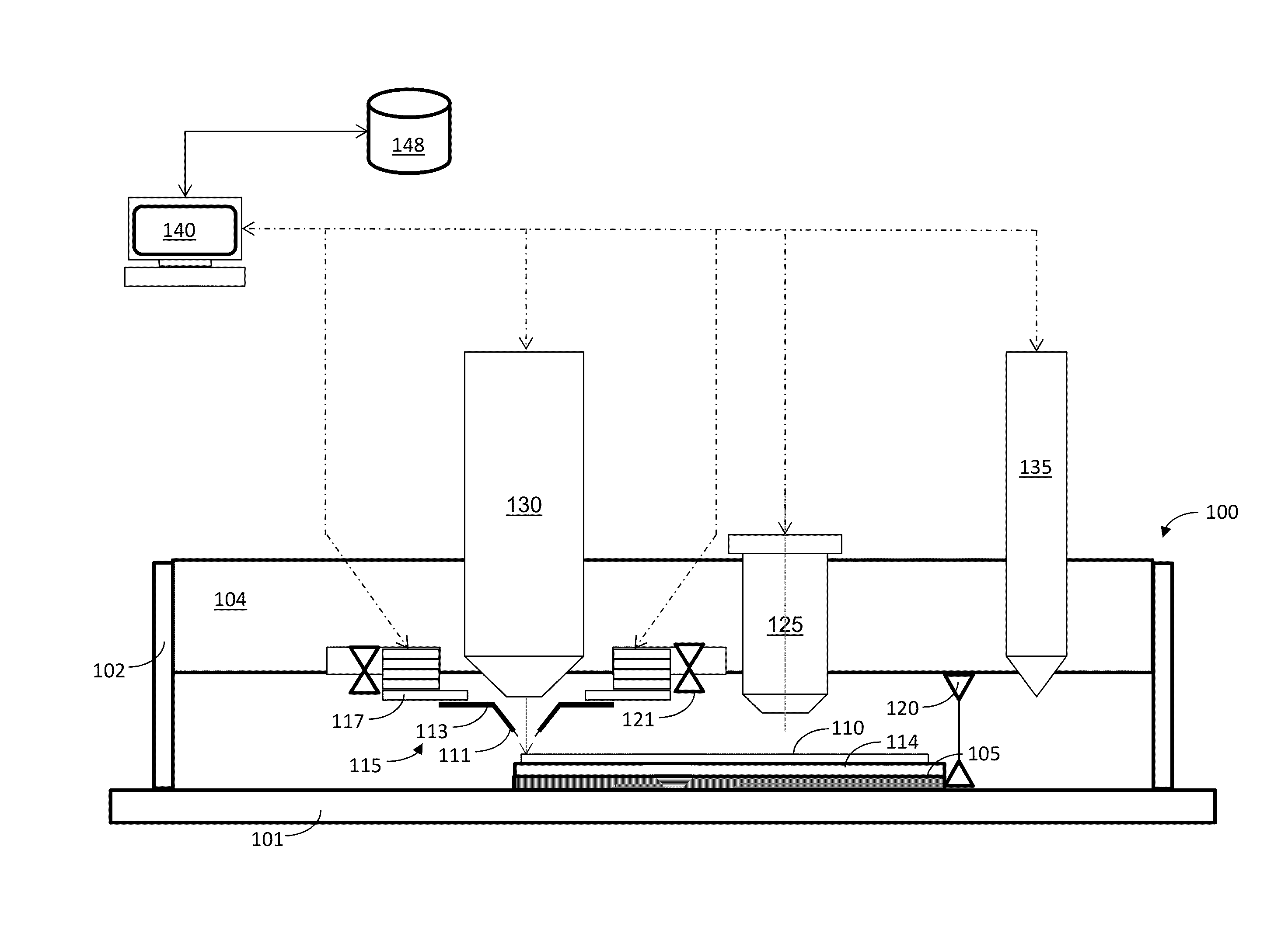
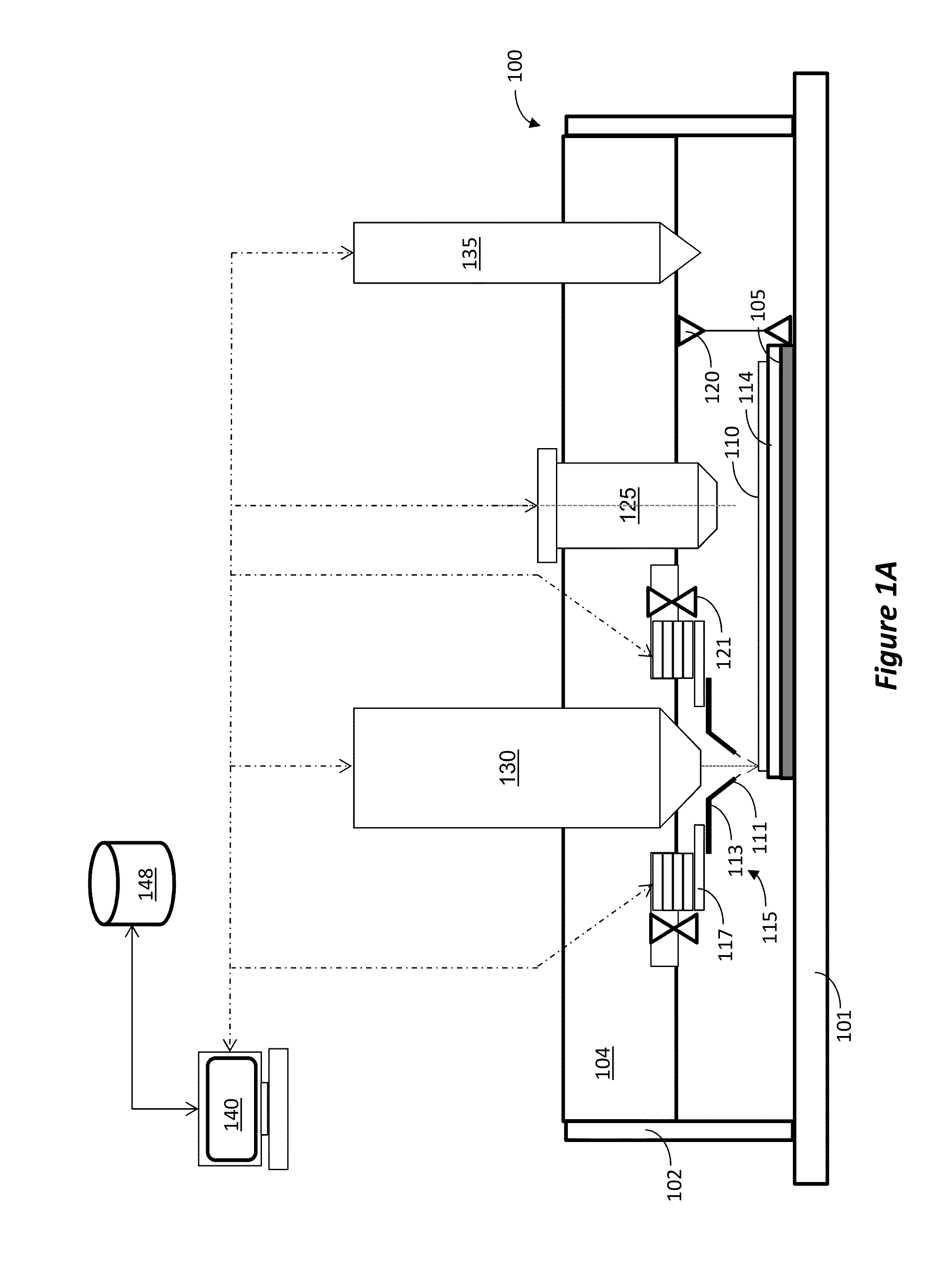
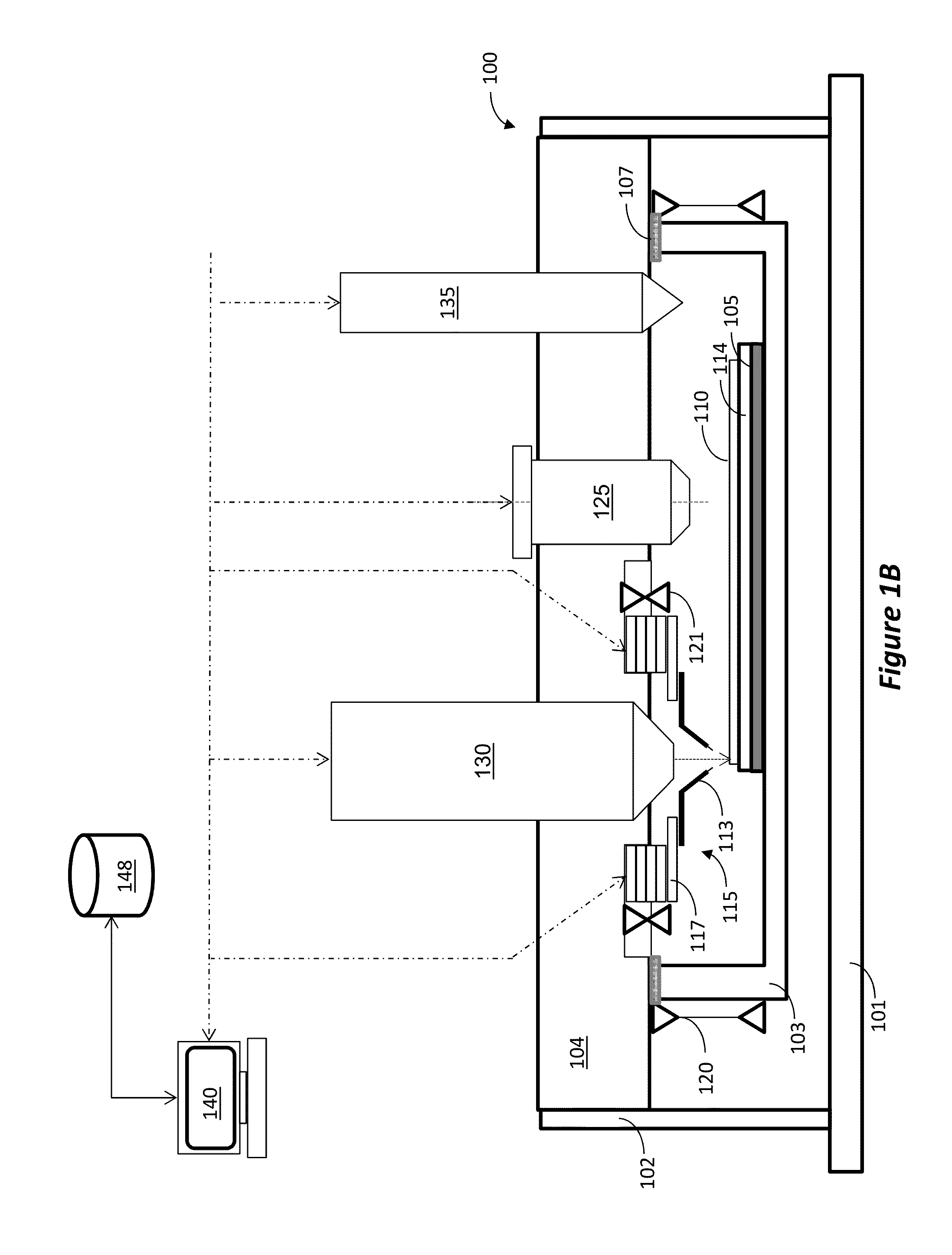
[0034]Using a scanning electron microscope (SEM) for imaging assistance during nanoprobing should help to resolve: (a) sample-probe damage and imaging degradation problems related to using AFP probes for both AFM imaging and nanoprobing, (b) need of wafer modification to create metal / dielectric contrast, (c) need of additional wafer cleaning after CMP to improve AFM quality and reduce risk of probe contamination by particles during sample scanning (d) reduce target acquisition time. However, to provide process control SEM-based nanoprobing should be done on wafer-size sample, on intra- and inter-chip level, in-line at different steps of process flow with negligible degree of damage, contamination and chip / device modification and multiple and safe returns of wafer back to manufacturing line.
[0050]The disclosed embodiments for integration of a wafer level SEM and a nanoprobe system incorporate system development for insertion of nanoprobe into an industrial quality SEM, while utilizing existing industry solutions of wafer handling and navigation and focus. Utilizing an existing industrial SEM immediately brings solution for two problems of in-line prober implementation: (1) probing of large wafer size samples and (2) fast, accurate and fully automated navigation on wafer. Use of industrial SEM for wafer handling and navigation is a significant step toward high-throughput recipe driven nanoprobing since existing industrial systems provide an excellent (a few seconds) move-acquire-measure (MAM) time.

Problems solved by technology

However, when the process does break or drift and factory yield goes down, process engineers need to perform failure analysis (FA) to investigate the failure and find out what process failed.
Recently; however, this approach began failing and, due to increasing fabrication complexity, the approach's failure rate is predicted to increase.
As a result, yield and process engineers confront a new challenge of finding a root cause of failure with less and less physical and dimensional information available for them.
Unfortunately, the electrical data become available only when at least one level of interconnect is formed.
This takes time and resources, and often causes scrap of many expensive wafers.
If a problem occurred during the front end fabrication steps and was not detected during that time, many wafers are scrapped.
The present front end monitoring tools often find defects which do not affect electrical performance and, otherwise, miss defects which do impact performance.
Many of these “killer” and performance defects would be discovered early-on if electrical measurements were made early in the process flow.
In practice, electrical tests are performed using specially designed test structures, wherein almost all electrical test structures are located in scribe line because IC real estate is very expensive, especially on production chips.
The test structures, being on the scribe lines and not the actual chip, do not properly reflect the electrical performance of the actual devices within the chip.
In both cases it requires additional wafer processing including expensive high-resolution patterning of the top or bottom layers.
The additional processing and de-processing of wafers increase the risk of misprocessing and wafer scrap.
In both cases placement of large test structures (standard test structure has 40 contact pads, each one of them with dimensions 50×50 um2 or more) is limited by high cost of wafer and chip real estate.
For instance, it is difficult to imagine placement of several test structure across chip e.g., to test macro-loading effects.
Also use of standard electrical test structures is limiting investigation of micro-loading effects since test structures have specific layout.
Both approaches are too complex or / and risky to try to implement them step by step through process flow.
In other words, these methods can be used occasionally and most likely off-line to solve complex monitoring problems but it is very hard to imagine that these methods will be used routinely, in-line for process monitoring and control.
This is just impractical.
Unfortunately, implementation of in-line AFP for wafer-size samples has several significant obstacles, some examples are as follows.
Poor AFP spatial resolution caused by damaged dull probes.
As a result, to date no wafer level in-line nanoprobing device has been developed.
These expensive off-line techniques are used today for technology development, ramp up and even manufacturing control.
These systems; however, cannot be used to test chips within wafers and cannot be used in-line.
However, the samples used in such devices are extremely small, compared to semiconductor wafers.
Therefore, use of such arrangement for in-line probing of wafers is not possible.
Thus, mounting the nanoprobe on the sample stage or on the sidewall door of an SEM vacuum chamber would mean that the nanoprobe can only test the other periphery of the wafer, but would not be able to reach and area of interest interior to the wafer.
Remaining problems with in-line AFP approach include:Particle generation and wafer contamination,Limited reach of nanoprobe fork,Travel and landing speed of nanoprobe,slow target acquisition of nanoprobe,IC contact damage (smearing),Poor AFP spatial resolution caused by damaged dull probes,Required by AFP wafer modification and deviation from the standard process flow (interlayer dielectric etching, corroded contact cleaning, etc.).
Problems with SEM-based nanoprobing implementation include:Lack of wafer size sample SEM-based nanoprobe design,Insufficient speed, precision and accuracy of on sample navigation,Unacceptable high level of thermal and mechanical probe vs. sample drift,Lack of force control during nanoprobing (for damage and particle free operation),Insufficient automation for hands-free recipe driven nanoprobing,Lack of reliable automated electrical data assessment, acceptance and evaluation,Long navigation, sample surface approach and data collection time (low throughput).< / ul

Method used


Image

  • Through process flow intra-chip and inter-chip electrical analysis and process control using in-line nanoprobing
  • Through process flow intra-chip and inter-chip electrical analysis and process control using in-line nanoprobing
  • Through process flow intra-chip and inter-chip electrical analysis and process control using in-line nanoprobing

Examples


Embodiment Construction

[0066]FIGS. 1A-1C illustrate various embodiments for the integration of in-line wafer level nanoprobe 115 with a wafer level SEM 130. The SEM can be used for standard SEM imaging of the region of interest (ROI) and for navigation and landing of the nanoprobes 115, including, in some embodiments, real time feedback for navigation and landing assistance. The nanoprobes may be used to perform parametric testing and characterization of the devices (e.g., transistors) within the ROI. Additionally, the SEM can be used to image the ROI while the nanoprobes are operated to perform the testing. For example, the nanoprobes may be used to drive current into the devices in the ROI, thereby changing the potential in certain areas of the ROI. The change in potential will cause a change in the SEM image. Similarly, certain shorts or resistance areas will cause a localized increase in temperature, which may also be visible in an SEM image. However, to achieve these objectives, the nanoprobes should...


PUM


Abstract

System for performing in-line nanoprobing on semiconductor wafer. A wafer support or vertical wafer positioner is attached to a wafer stage. An SEM column, an optical microscope and a plurality of nanoprobe positioners are all attached to the ceiling. The nanoprobe positioners have one nanoprobe configured for physically contacting selected points on the wafer. A force (or touch) sensor measures contact force applied by the probe to the wafer (or the moment) when the probe physically contacts the wafer. A plurality of drift sensors are provided for calculating probe vs. wafer alignment drift in real-time during measurements.

Description

RELATED APPLICATION[0001]This application claims priority benefit from U.S. Provisional Application, Ser. No. 62 / 016,650, filed Jun. 25, 2014, the disclosure of which is incorporated herein in its entirety.BACKGROUND[0002]1. Field of Invention[0003]This invention is in the field of semiconductor manufacturing and, more specifically, enabling electrical measurements via nanoprobing at wafer level process monitoring to accomplish in-line monitoring, defect review and process control.[0004]2. Related Art[0005]Process engineers always tried to get as much information as possible about devices and circuits they built. Device information can be divided into two groups: physical and electrical characteristics. Electrical characteristics give the ultimate properties of the fabricated device and, if these conform to the design, nothing else is really needed for process monitoring and control. Certainly, electrical characteristics would be sufficient if a process never breaks or drifts over t...

Claims


Application Information

Patent Timeline
Patent Type & Authority Applications(United States)
IPC IPC(8): G01Q30/02G01R31/28G01R31/26
CPCG01Q30/02G01R31/2891H01J37/28H01J2237/2008H01J2237/208H01L22/14G01R31/26G01R1/06744G01R31/2831H01L22/12H01J2237/2817G01R31/2601
Inventor UKRAINTSEV, VLADIMIRNIV, ISRAELBENZION, RONEN
Owner DCG SYST
Why Eureka
Try Eureka