Methods and apparatus for the fabrication of pattern arrays in making touch sensor panels

a technology of pattern arrays and touch sensors, applied in the direction of lamination ancillary operations, instruments, computing, etc., can solve the problems of film shrinkage, though greatly reduced, still observed, and increase the conductivity of ito, so as to reduce the error associated with coating alignment, improve the resulting registration of the conductive array, and improve the effect of registration and alignmen

Inactive Publication Date: 2016-01-07
PRECO
View PDF0 Cites 21 Cited by
  • Summary
  • Abstract
  • Description
  • Claims
  • Application Information

AI Technical Summary

Benefits of technology

[0026]The present disclosure relates to methods for improving registration and alignment between the sense and drive layers of a touch sensor panel wherein the conductive layers are laser patterned after fabrication of the sensor panel. Laser patterning both conductive coatings, wherein the conductive coatings are in a fixed orientation or position with respect to one another prior to laser patterning, whether laminated together or coated on to opposing sides of a single substrate, reduces the error associated with alignment of the coatings. This allows for a greater increase in the resulting registration of the conductive array, increasing the sensitivity of the touch panel. The method utilizes a laser system not requiring changing of settings to pattern each layer and further minimizes alignment and registration problems related to substrate shrinkage or warping prior to lamination and the prior art method problems including matching of the patterned layers when subsequently laminated together.

Problems solved by technology

First, the conductivity of ITO increases and conduction variability reduces over the surface after annealing.
Unfortunately, film shrinkage, though greatly reduced, is still observed when the film is subjected to the many processing steps after annealing.
When the drive and sensor layers are produced separately and the production is in large scale, tracing and matching production lots become a very difficult task.
Presently, the most difficult step in preparing a sensor is laminating the drive layer to the sense layer.
For any reasonable sensor size larger than approximately 15 cm, this becomes a challenging task since the challenge in registration not only comes from the machine alignment accuracy within this lamination step, but also from the adjustment of the cumulative dimensional errors in both films resulting from the many processing steps prior to this lamination step.
These errors can result from the imaging process during etching of the electrodes, shrinkage of the film during oven-drying after each of the two printing steps, and / or tension-induced stretch on the film during film transport and lamination.
As the size of the sensor becomes larger, it becomes extremely difficult to meet the required specification if the drive and sensor layers are laminated late in the fabrication process.
The greater the number of processes and the more equipment involved in the process of forming the pattern, the greater the cumulative dimensional error.
The more the two layers are processed separately, the more difficult it is to compensate for the errors when the layers are combined.
In addition, the increase in the number of times a liner is removed before processing and a new liner re-applied after processing, the greater the chance the film has been exposed to dust and debris.
Further, as the sensor surface size increases, so do the issues relating to dimensional error, making it much more difficult to form a debris-free panel.
The ITO coated conductive material also presents other difficulties when the touch panel size increases.
This not only reduces the optical transparency of the panel but also reduce the flexibility in handling the material as a thicker ITO layer is brittle and subjected to micro-crack during handling and the fabrication process.

Method used


Image

  • Methods and apparatus for the fabrication of pattern arrays in making touch sensor panels
  • Methods and apparatus for the fabrication of pattern arrays in making touch sensor panels
  • Methods and apparatus for the fabrication of pattern arrays in making touch sensor panels

Examples


example 1

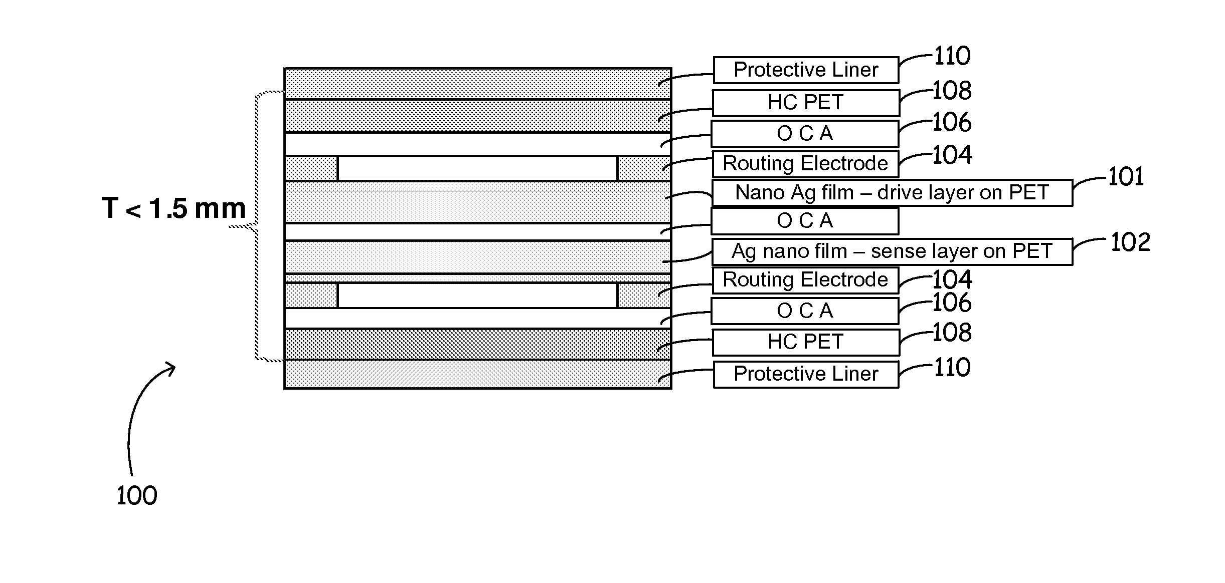
[0055]A touch panel 100 made from silver nanowire conductors having a layer construction as illustrated in FIG. 9 may be fabricated by the method of the present disclosure. The panel construction is similar to the construction illustrated in FIG. 3, except the conductive coatings are instead conductive coatings comprising silver nanowires (in contrast to ITO). In this example, the silver nanowires are solution-coated with PMMA (Polymethylmethacrylate (Acrylic)) binder. Typical binder thickness is approximately 6 μm. The substrate is PET (Polyethylene Terephthalate), having typical substrate thickness of approximately 100 μm. The conductive layers may be separated by an insulator, for example, an insulting layer such as a substrate or an adhesive layer in order for the electrically conductive array to function as a touch sensor.

[0056]The method of fabricating the laminate construction, or touch sensor panel, according to the present disclosure is distinct over the prior art processes...

example 2

[0068]A touch panel 200 made from silver nanowires conductors having a layer construction as illustrated in further detail in FIG. 11 may be fabricated as follows: the silver nanowires are spin-coated with PMMA binder sequentially onto both sides of a 400 μm PC substrate. The PMMA binder has a thickness of approximately 6 μm. A 2.15 μm laser can be used for patterning the electrical arrays on both conductive coatings, on both sides of the substrate. For a double-side coated substrate, no lamination is necessary before laser patterning the conductive layers as once each layer is coated onto a respective, opposing side of a substrate, the layers are in a fixed orientation with respect to one another. FIG. 12 illustrates these simplified processing steps. Processing steps 212 to 242 are illustrated in FIG. 12 and include, for example, coating the nanowire silver film on to both sides of a PC substrate 212; laser imaging on both the drive and sense layers 216, printing a silver ink on t...

example 3

[0071]A silver nanowire coated PET film is normally received with a 50 μm thick PE (Polyethylene) release liner on top to protect the coating surface. By providing better intimate contact between the release liner and the film and by placing the film under a scanning 1.04 μm laser without removing the liner, terminating score lines were formed on the conducting layer, similar to lines obtained when processing with the protective liner removed. Upon removing the liner after imaging, no smoke, debris or other damages were observed on the film surface after visual inspection under a microscope at 90× power. Unlike the conventional patterning methods with generally include litho / etch wet processes or laser ablating / evaporation processes where the liner must be removed, the current laser patterning process can be conducted without the removal of the protective liner. No post cleaning step nor application of new protective liner is required. In Examples 1 and 2 wherein a 2.15 μm laser may...


PUM

PropertyMeasurementUnit
wavelengthaaaaaaaaaa
sizeaaaaaaaaaa
widthaaaaaaaaaa

Abstract

An electrically conductive touch sensor panel construction and method and laser system for fabricating the same. The transparent touch sensor panel comprises at least two conductive coatings to provide a drive layer and a sense layer. The drive and sense layers are laminated together or otherwise assembled in a touch panel construction and in selected alignment. The layers are then subsequently laser patterned to form the conductive pathways for the touch panel sensor. The drive and sense layers may be concurrently or sequentially laser processed to form a selected pattern in each layer such that the drive and sense layers are substantially aligned forming a far more precise pattern array for the panel.

Description

CROSS-REFERENCE TO RELATED APPLICATIONS[0001]The present application is based on and claims the benefit of U.S. provisional patent application Ser. No. 62 / 019,696, filed Jul. 1, 2014 and U.S. provisional patent application Ser. No. 62 / 039,606, filed Aug. 20, 2014, the contents of which are hereby incorporated by reference in their entirety.FIELD OF THE INVENTION[0002]This invention relates generally to the fabrication of touch sensor panels. More specifically, it relates to the methods and systems for the fabrication of the electrical pattern arrays for touch sensors made from silver nanowire coated conductive films. It offers novel techniques for processing larger touch panels with better sensor accuracy, improved registration of the conductive layers and fewer fabrication and processing steps and higher throughput.BACKGROUND OF THE INVENTION[0003]A touch screen is an input device often used in conjunction with another functional device. For example, a transparent touch screen with...

Claims


Application Information

Patent Timeline
Patent Type & Authority Applications(United States)
IPC IPC(8): B29C65/00G06F3/041
CPCB29C65/002B29L2031/723G06F2203/04103G06F3/041G06F2203/04112G06F3/0445G06F3/0446
Inventor CHOW, CHRISTOPHERMILLER, DANIEL B.BUCKLEW, JAMES J.POULAIN, DANASCHUSTER, RANDYPIERSON, JR., JOHN T.
Owner PRECO
Why Eureka
Try Eureka