Semiconductor device and method of forming the same

Active Publication Date: 2016-01-21
UNITED MICROELECTRONICS CORP
View PDF5 Cites 17 Cited by
  • Summary
  • Abstract
  • Description
  • Claims
  • Application Information

AI Technical Summary

Benefits of technology

[0007]The invention is directed to a semiconductor device and a method of forming the same. Specifically, a tri-layer spacer structure is formed on a sidewall of a gate, wherein

Problems solved by technology

However, due to the increasing level of integration of the devices, the minimization of the device dimension reaches its limitations.
Unfortunately, the integration of the SiGe/SiC strain layer into the CMOS ma

Method used


Image

  • Semiconductor device and method of forming the same
  • Semiconductor device and method of forming the same
  • Semiconductor device and method of forming the same

Examples


Embodiment Construction

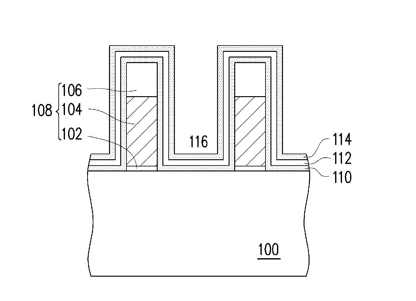
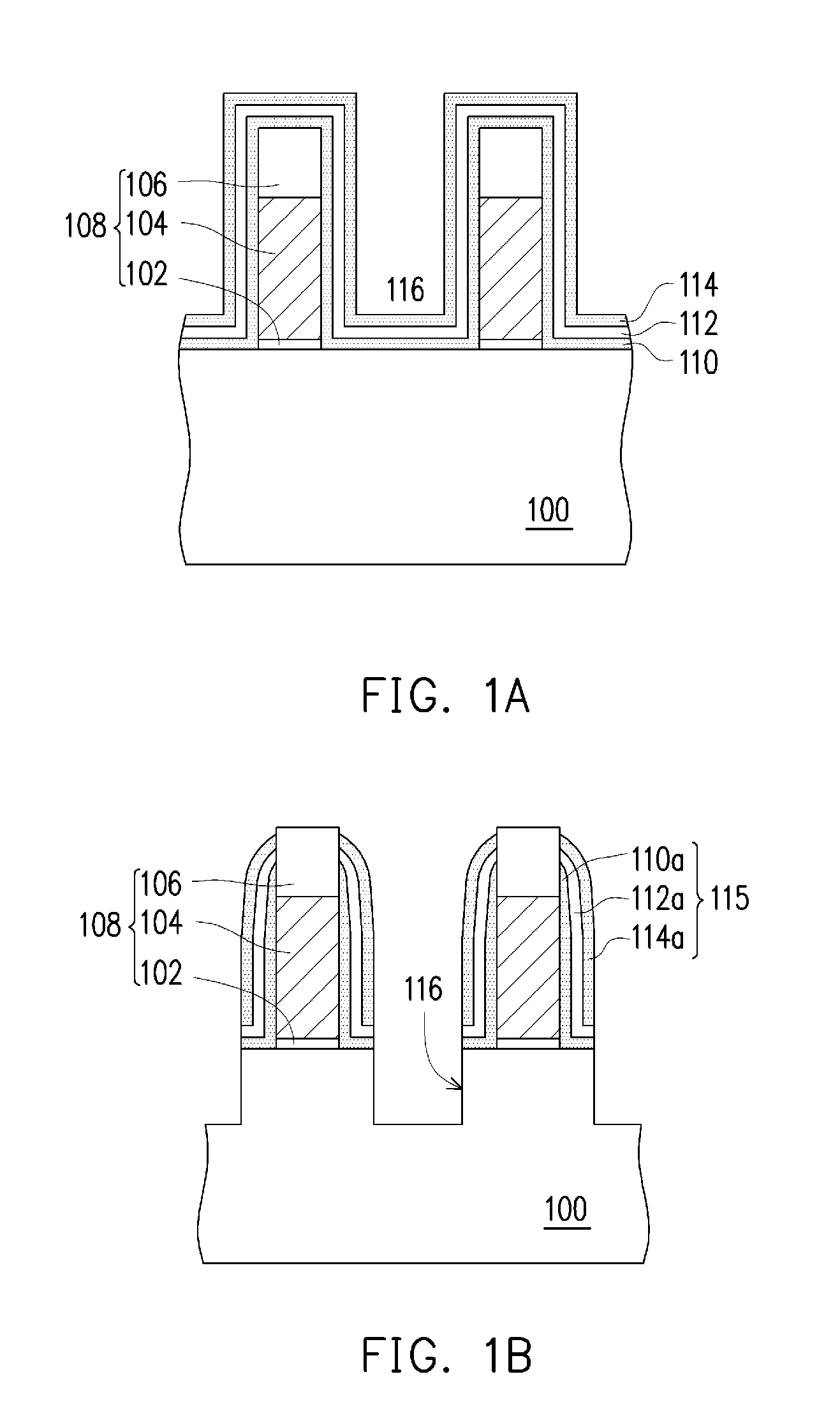
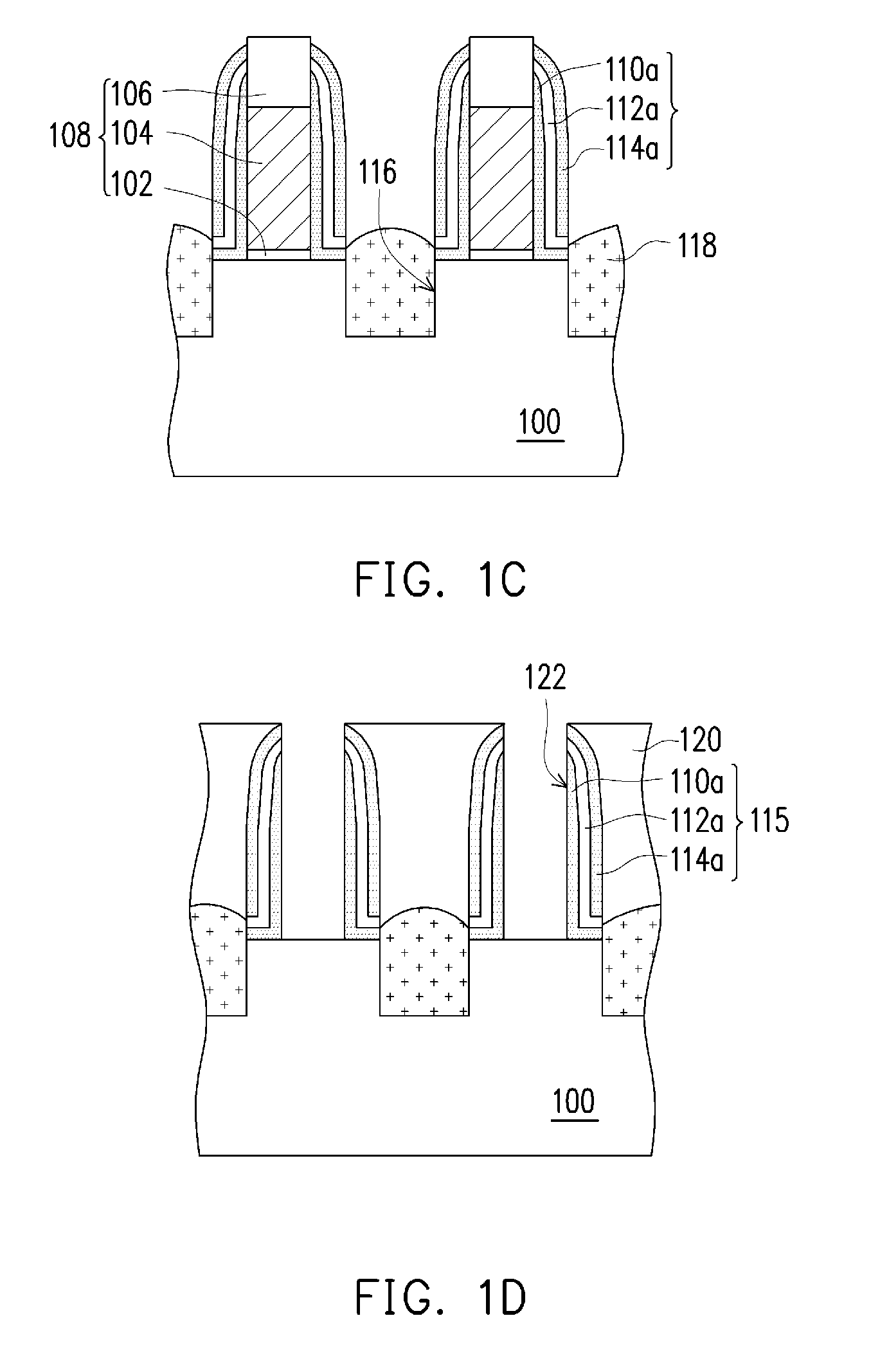
[0031]FIG. 1A to FIG. 1D are schematic cross-sectional views illustrating a method of forming a semiconductor device according to an embodiment of the invention.

[0032]With reference to FIG. 1A, at least one stacked structure 108 is provided on a substrate 100. The substrate 100 is a semiconductor substrate, e.g., a silicon substrate. Each stacked structure 108 includes an interfacial layer 102, a gate 104, and a cap layer 106 sequentially disposed on the substrate 100. The interfacial layer 102 includes silicon oxide, silicon nitride, a high-k material with a dielectric constant greater than 4, or a combination thereof. The high-k material can be metal oxide, e.g., rare-earth metal oxide. Besides, the high-k material can be selected from the group consisting of hafnium oxide (HfO2), hafnium silicon oxide (HfO2), hafnium silicon oxide (HfSiO4), hafnium silicon oxynitride (HfSiON), aluminum oxide (Al2O3), lanthanum oxide (La2O3), tantalum oxide (Ta2O5), yttrium oxide (Y2O3), zirconium...


PUM


Abstract

A method of forming a semiconductor device is provided. At least one stacked structure is provided on a substrate. A first spacer material layer, a second spacer material layer, and a third spacer material layer are sequentially formed on the substrate and cover the stacked structure. The first, second, and third spacer material layers are etched to form a tri-layer spacer structure on the sidewall of the stacked structure. The tri-layer spacer structure includes, from one side of the stacked structure, a first spacer, a second spacer, and a third spacer, and a dielectric constant of the second spacer is less than each of a dielectric constant of the first spacer and a dielectric constant of the third spacer.

Description

CROSS-REFERENCE TO RELATED APPLICATION[0001]This application claims the priority benefit of Chinese application serial no. 201410341635.8, filed on Jul. 17, 2014. The entirety of the above-mentioned patent application is hereby incorporated by reference herein and made a part of this specification.BACKGROUND[0002]1. Field of the Invention[0003]The invention relates to an integrated circuit and a method of forming the same, and more particularly, to a semiconductor device and a method of forming the same.[0004]2. Description of Related Art[0005]In the field of integrated circuit devices, the device dimension is often reduced to ensure high operating speed and low power consumption. However, due to the increasing level of integration of the devices, the minimization of the device dimension reaches its limitations. One proposed solution to overcome the limitations imposed by said device miniaturization is strain engineering.[0006]Strain engineering is to utilize materials with the same...

Claims


Application Information

Patent Timeline
IPC IPC(8): H01L21/308H01L29/78
CPCH01L21/3086H01L29/7848H01L21/3081H01L29/66545H01L29/6656H01L29/66636H01L29/78
Inventor LU, MAN-LINGHUNG, YU-HSIANGCHANG, CHUNG-FUWU, YEN-LIANGSHEN, WEN-JIUNLIU, CHIA-JONGFU, SSU-ICHEN, YI-WEI
Owner UNITED MICROELECTRONICS CORP
Why Eureka
Try Eureka