Flexible fingerprint sensor materials and processes

Active Publication Date: 2016-01-28
GLOBAL GRAPHENE GRP INC
View PDF2 Cites 90 Cited by
  • Summary
  • Abstract
  • Description
  • Claims
  • Application Information

AI Technical Summary

Benefits of technology

[0017]In an embodiment, the flexible substrate contains a thin layer of polymer that is preferably 1-50 μm thick, more preferably 1-20 μm, and most preferably 1-10 μm. This flexible polymer may be selected from a polyester (e.g. polyethylene terephthalate (PET), polyethylene naphthalate (PEN), and polyester ionomer), polyethersulfone (PES), polycarbonate (PC), polysulfone, a phenolic resin, an epoxy resin, polyimide, polyether ester, polyetheramide, cellulose nitrate, cellulose acetate, poly(vinyl acetate), polystyrene, polyolefins including polyolefin ionomers, polyamide, aliphatic polyurethane, polyacrylonitrile, polytetrafluoroethylene, polyvinylidene fluoride, poly(methyl methacrylate), an aliphatic or cyclic polyolefin, polyarylate (PAR), polyetherimide (PEI), polyethersulphone (PES), polyimide (PI), Teflon poly(perfluoro-alboxy) fluoropolymer (PFA), poly(ether ether ketone) (PEEK), poly(ether ketone) (PEK), poly(ethylene tetrafluoroethylene) fluoropolymer (PETFE), poly(methyl methacrylate), an acrylate/methacrylate copolymer (PMMA), natural or synthetic paper, resin-coated or laminated paper, or a combination thereof. In a preferred embodiment, the flexible substrate is polyimide or a copolymer the

Problems solved by technology

This type of sensor has the disadvantage that the imaging capabilities are affected by the quality of skin on the finger.
For example, a dirty or marked finger is difficult to image properly.
However, unlike capacitive sensors, this sensor technology is not susceptible to electrostatic discharge damage.
These rigid components are incompatible with flexible electronics (e.g. the bendable flexible smart phone or wearable device).
All these individual components are very rigid and unfit for a flexible device design.
However, the flexible substrate (polymer) based fingerpri

Method used


Image

  • Flexible fingerprint sensor materials and processes
  • Flexible fingerprint sensor materials and processes

Examples


example 1

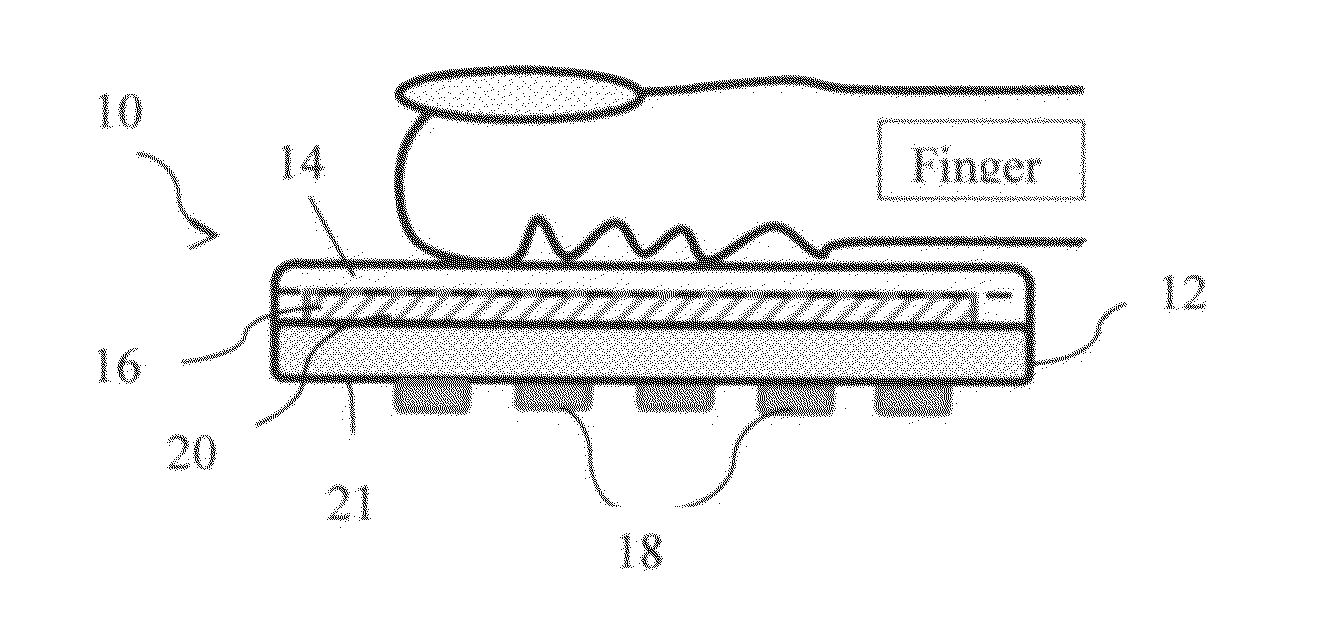
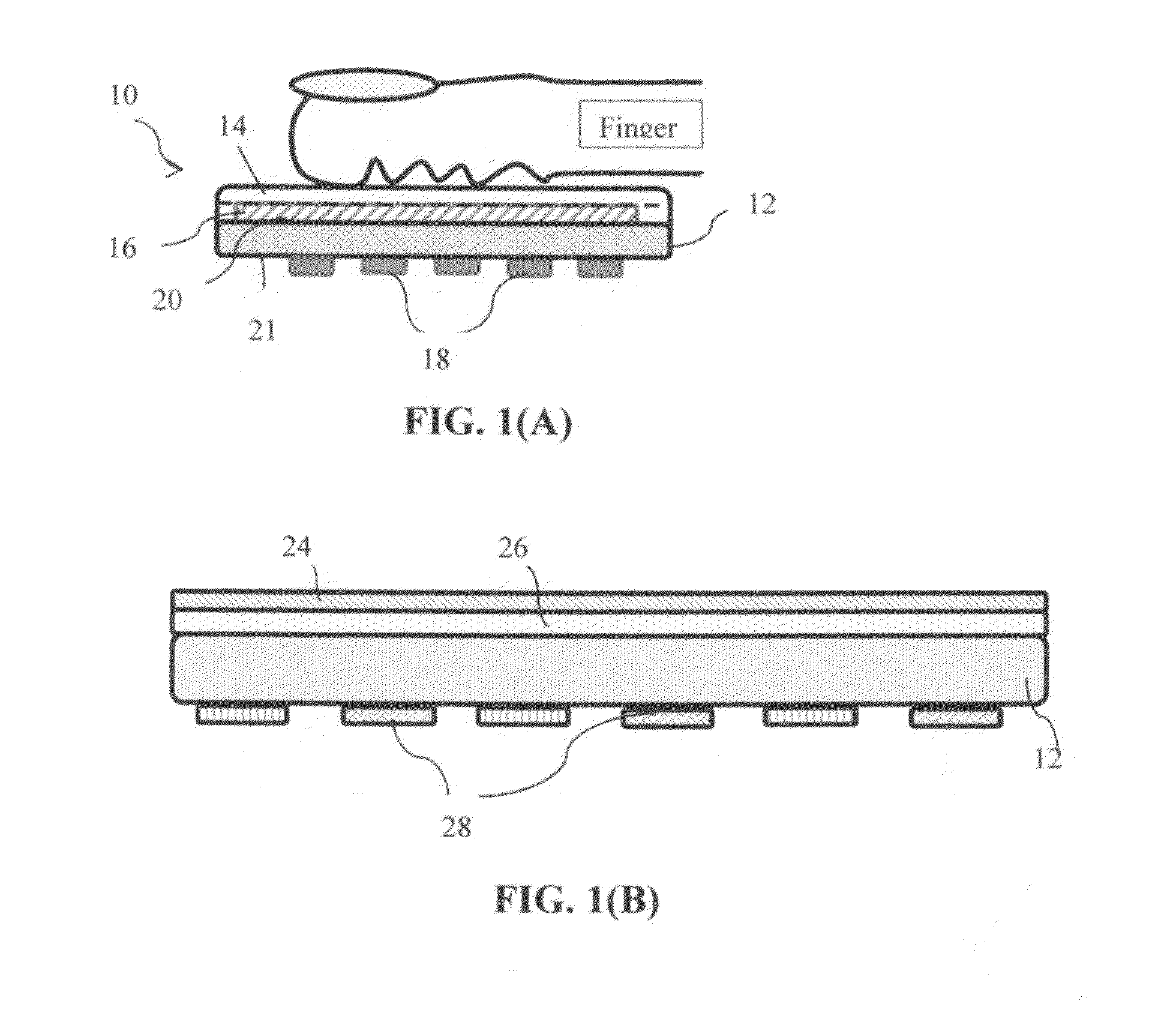
Layer (Domains) of a Conductive Material with No Coverage by a Protective Hard Coating

[0069]A typical procedure of producing a flexible laminate for a fingerprint sensor is described as follows: In one example, approximately 0.249 g of multi-layer graphene sheets (supplied by Angstron Materials, Inc., Dayton, Ohio, USA) was added to 2.25 g, 1.125% HPMC (Hydroxypropyl Methyl Cellulose) and then mixed with 0.35 g PES 20 (polyether sulfone) solution and 1.45 g, 1.5% silver nanowires (AgNW) to produce a conductive dispersion (suspension). The resulting suspension has a concentration of 5.8% graphene, 8.14% PES 20, 33.7% AgNW, 13% IPA, 38.7% H2O.

[0070]To prepare conductive films on polyimide (PI) substrates, we treated substrates with UV / Ozone or corona to make a low surface energy surface for improved wetting by the suspension when coated thereon and for improved adhesion between the substrate and graphene-AgNW conductive layer. The conductive dispersion was deposited onto the PI film b...

example 2

Layer of a Conductive Material with a Protective Hard Coating

[0073]In this series of examples, a thin layer of resin or resin-filler composite was applied as a protective hard coating. In this series, the suspension of graphene (or MWCNT, other fibrous conductive fillers) and the suspension of metal nanowires (AgNW or CuNW) or carbon nanotube / fiber (CNT or CNF) were prepared separately. For instance, 3.03 g graphene was dispersed in 30.07 g PET resin (Hank RZ 570) to produce a suspension having a graphene concentration of 9.15% by weight mixed with 90.85% PET resin. This is herein referred to as Suspension A. A suspension of AgNW or CuNW in a liquid mixture of methanol and water (Methanol: H2O=1:1) was prepared to produce a nanowire concentration of 0.065% by weight. This is referred to as Suspension B. Two mixing / coating routes were then followed: (a) Suspension A and Suspension B are mixed first, followed by coating onto a solid substrate surface; (b) Suspension A and Suspension B...

example 3

Spray-Coated Conductive Layers Covered by a UV-Cured Protective Coating

[0077]In one of this series of samples, graphene dispersion (Suspension A) was prepared by dispersing 3.03 g of graphene (Angstron N006) in 30.07 g PET resin (Hank RZ 570), which was diluted with 15.8 g IPA and 31.6 g H2O to produce a suspension with a graphene concentration of 3.76%, and PET resin of 37.3%. Suspension B was made in a way similar to that in Example 2 to produce a suspension containing a 0.065% concentration of AgNW in liquid medium (Methanol: H2O=1:1). Suspension C was obtained by mixing 0.2 g epoxy resin (K-500) with 3.31 g acrylic resin (R44-234) in 8.83 g of a co-solvent, forming a 1.62% concentration of UV-curable hard coat resin.

[0078]To prepare conductive graphene films on solid substrates, the substrate was treated with UV / Ozone to make low surface energy surface for graphene spray-coating layer. In one example, graphene dispersion (Suspension A) was spray-coated on the PI film. Then, AgNW...


PUM


Abstract

A flexible fingerprint sensor laminate comprising: a layer of flexible substrate having a front surface and a back surface, at least a domain of electrically conductive material deposited on the front surface, a protective hard coating layer that covers the domain of electrically conductive material, and a plurality of sensor electrodes deposited preferably on the back surface and related circuitry (e.g. integrated circuit for driving and sensing). Preferably, the layer of flexible substrate is no greater than 20 μm in thickness, the domain of electrically conductive material has a thickness no greater than 2 μm, the protective hard coating has a thickness no greater than 1 μm, and the laminate has a surface sheet resistance no greater than 200 Ohm per square and surface scratch resistance no less than 3 H. The laminate exhibits good scratch resistance, low sheet resistance, good flexibility and mechanical integrity. The invention also provides a biometric sensor, such as a fingerprint sensor. The invention further provides a process for producing such a sensor laminate.

Description

FIELD OF THE INVENTION[0001]The present invention relates to the field of fingerprint sensors for personal identification and verification and, more particularly, to fingerprint sensor materials and processes.BACKGROUND OF THE INVENTION[0002]Fingerprint sensing and matching is widely used for personal identification or verification. A common approach to fingerprint identification involves scanning a sample fingerprint or an image thereof and storing the image and / or unique characteristics of the fingerprint image. The characteristics of a sample fingerprint may be compared to information for reference fingerprints already stored in a database to determine or verify identification of an individual.[0003]A fingerprint sensor is an electronic device used to capture a digital image of the fingerprint pattern. The captured image is called a live scan. This live scan is digitally processed to create a biometric template (a collection of extracted features) which is stored and used for mat...

Claims


Application Information

Patent Timeline
IPC IPC(8): G06K9/00H01L21/283
CPCG06K9/00053G06K9/0002H01L21/283G06V40/1329G06V40/1306
Inventor LIN, YI-JUNJANG, BOR ZLEE, SHAIO-YENZHAMU, ARUNA
Owner GLOBAL GRAPHENE GRP INC
Why Eureka
Try Eureka