Method of patterning dopant films in high-k dielectrics in a soft mask integration scheme

a technology of soft mask and integrated circuit, which is applied in the direction of semiconductor devices, basic electric elements, electrical equipment, etc., can solve the problems of cumbersome methods for forming gates of n- and p-type transistors, and achieve the effect of preventing adverse effects on tiny particles and improving performance in complementary metal oxides

Active Publication Date: 2016-01-28
IBM CORP
View PDF1 Cites 36 Cited by
  • Summary
  • Abstract
  • Description
  • Claims
  • Application Information

AI Technical Summary

Benefits of technology

[0030]The present invention improves performance in complementary metal oxide semiconductor (“CMOS”) technology integrated circuits by providing methods for doping the high dielectric constant, i.e., “high-k” gate dielectric layer, of an FET in a replacement metal gate integration scheme.
[0031]The present invention advantageously uses selective etching of multi-layered stacks containing a sacrificial film or controlled etching of single layered blocking stack to form high-k replacement metal gate structures made using soft metal mask without degradation of device properties of the transistors. The methods allow threshold differences to be created among different types of FETs or the same type of FET. Presented are doping methods using the stack as a buffer or blocking stack during doping. Another method is a direct doping method of the high-k using a multi-layered stack as a mask.
[0032]In one embodiment, herein referred to “embodiment A”, a blocking stack allows a replacement metal gate structure having one doped and one undoped high-k gate oxide to be formed in a first and second transistor, respectively. In the context of all the embodiments, the term “doping” refers to the incorporation of metal elements (such as, but not limited to, rare-earth elements like lanthanum) into the high-k gate dielectric film to change the effective work function of the transistor. The method uses a multi-layered blocking layer, which due to its multi-layers, may be initially thick and then later thinned. It is advantageous to have a thick layer when patterning using a soft mask to protect the underlying gate materials from damage during the soft-mask reactive ion etching (RIE) process. The patterning reveals the high-k material in a first FET which is to be doped and leaves the blocking stack on the second FET which is to remain undoped. After the soft mask

Problems solved by technology

However, differences in the workfunctions of NFET and PFET devices typically require different metal layers to be provided in the gat

Method used


Image

  • Method of patterning dopant films in high-k dielectrics in a soft mask integration scheme
  • Method of patterning dopant films in high-k dielectrics in a soft mask integration scheme
  • Method of patterning dopant films in high-k dielectrics in a soft mask integration scheme

Examples


Embodiment Construction

Indirect Doping

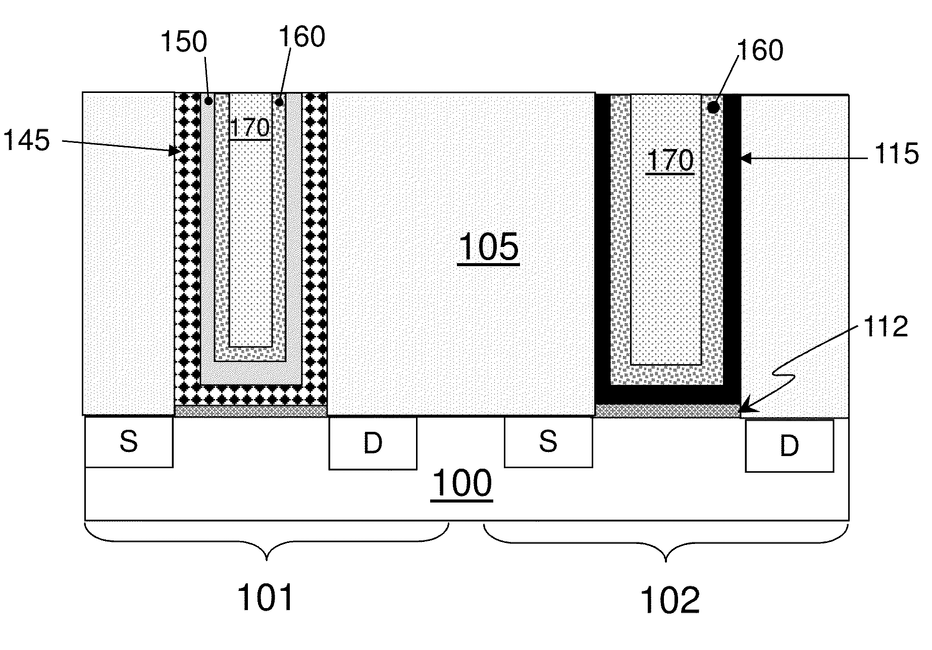
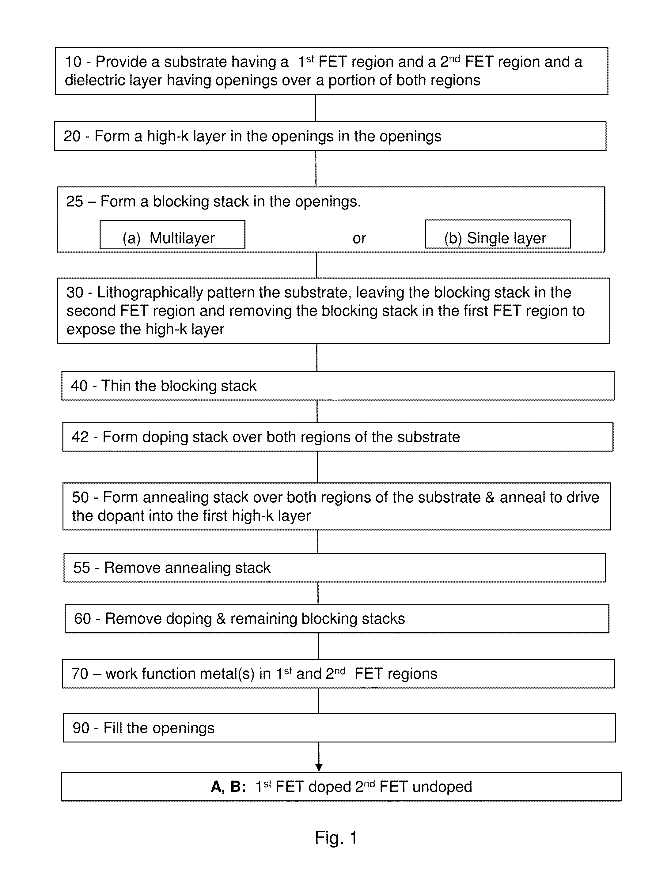
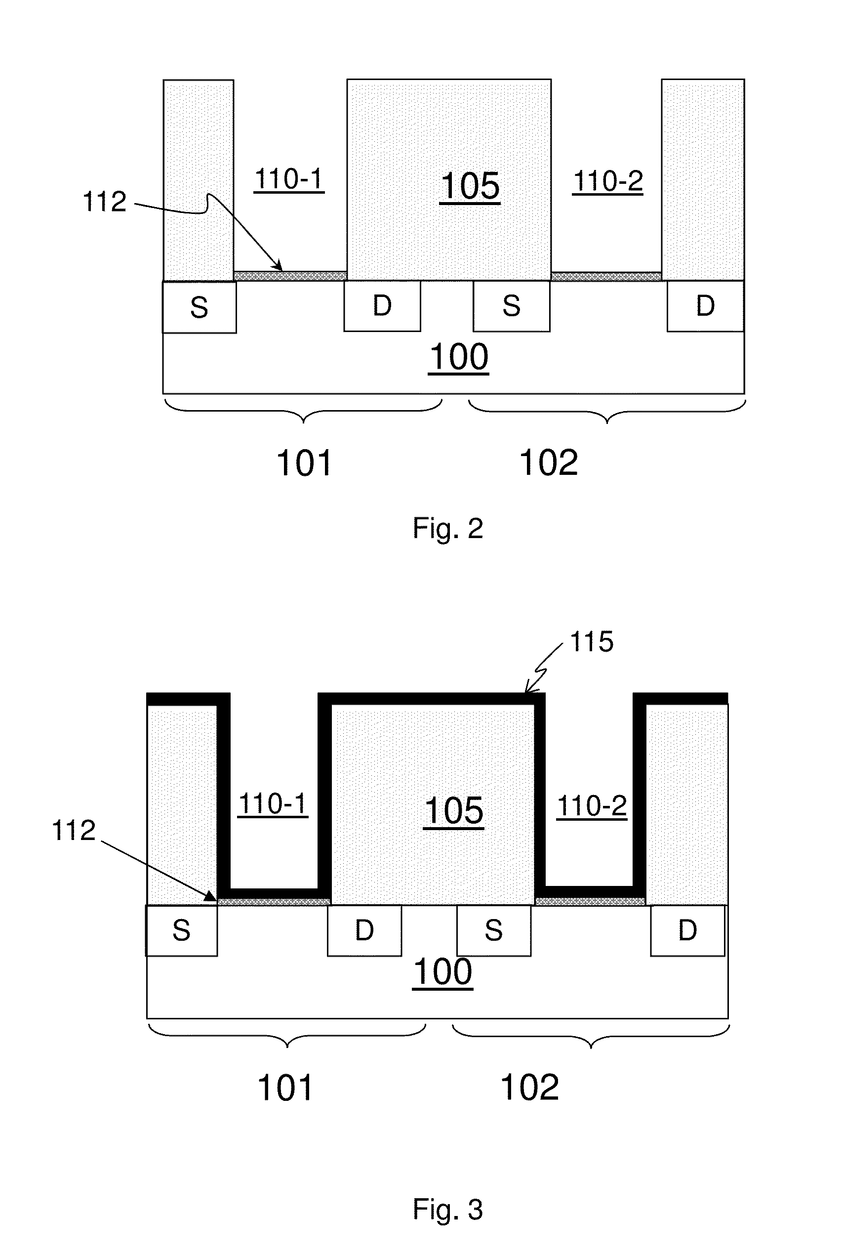
[0035]FIG. 1 is a flow chart of embodiments A and B of the present invention of making one doped and one undoped FET using a multi-layered blocking stack (embodiment A) or a single layer blocking stack (embodiment B) in a soft mask replacement metal gate process. In step 10 a substrate having an N-FET region and a P-FET region is provided. Over the substrate is a dielectric layer having two openings, which preferably were made by removing a dummy gate. These openings will be over the N-FET or P-FET region of the substrate and depending high-k integration scheme, may expose the substrate (“high-k last” integration scheme), may expose an interfacial layer in contact with the substrate (“high-k last” integration scheme), or may expose a high-k dielectric previously formed over the substrate (“high-k first” integration scheme). These openings will contain the future high-k, metal gates of the FETs.

[0036]Still referring to FIG. 1, in step 20, a high-k layer is formed in th...


PUM


Abstract

A method of fabricating advanced node field effect transistors using a replacement metal gate process. The method includes dopant a high-k dielectric directly or indirectly by using layers composed of multi-layer thin film stacks, or in other embodiments, by a single blocking layer. By taking advantage of unexpected etch selectivity of the multi-layer stack or the controlled etch process of a single layer stack, etch damage to the high-k may be avoided and work function metal thicknesses can be tightly controlled which in turn allows field effect transistors with low Tiny (inverse of gate capacitance) mismatch.

Description

BACKGROUND OF THE INVENTION[0001]The subject matter of the present application relates to semiconductor devices of integrated circuits and their fabrication, particularly field effect transistors.[0002]One of the ways proposed to improve performance in complementary metal oxide semiconductor (“CMOS”) technology integrated circuits is to provide a high dielectric constant, i.e., “high-k” gate dielectric layer, for n-type and p-type field effect transistors (“NFET” and “PFET” devices), and to form metal gates of the NFET and PFET devices.[0003]However, differences in the workfunctions of NFET and PFET devices typically require different metal layers to be provided in the gates of respective N- or P-type transistors. Heretofore, methods for forming the gates of N- and P-type transistors have been cumbersome. Further improvements in the fabrication of N- and P-type transistors having metal gates can be made.BRIEF DESCRIPTION OF THE DRAWINGS[0004]FIG. 1 is an illustrative flow chart of m...

Claims


Application Information

Patent Timeline
IPC IPC(8): H01L21/3213H01L21/28H01L21/321
CPCH01L21/32133H01L21/28229H01L21/28088H01L21/32135H01L21/32115H01L21/32139H01L21/28079H01L21/823462H01L21/02321H01L21/0273H01L21/0332H01L21/225H01L21/28185H01L21/28194H01L21/31111H01L21/31116H01L21/31144H01L21/3115H01L21/32134H01L21/324H01L21/823437H01L21/82345H01L21/823842H01L21/823857H01L29/4966H01L29/513H01L29/517H01L29/66545
Inventor ANDO, TAKASHIJAGANNATHAN, HEMANTHKANNAN, BALAJIKRISHNAN, SIDDARTH A.KWON, UNOHRAJARAM, REKHA
Owner IBM CORP
Why Eureka
Try Eureka