Optical emission collection and detection device and method

a detection device and optical emission technology, applied in the direction of fluorescence/phosphorescence, instruments, material analysis, etc., can solve the problems of simple focusing lens not being able to determine the suitable emission angle information, generating unwanted optical interference, and affecting the signal quality of the collection, so as to minimize optical aberration, minimize the effect of blurring effect, and increase the signal-to-noise ratio of the collection emission signal

Inactive Publication Date: 2016-02-04
FLIR DETECTION
View PDF4 Cites 7 Cited by
  • Summary
  • Abstract
  • Description
  • Claims
  • Application Information

AI Technical Summary

Benefits of technology

[0024]The current invention can use a fluorescence collection optical system of the type having an ellipsoidal reflector. An emission source is optically positioned at the first foci of the ellipsoidal reflector. The emission source preferably comprises a surface plasmon coupled emission slide and fluorescence material coated on a reacting side of the surface plasmon coupled emission slide. The surface plasmon coupled emission slide is preferably a multilayered slide that is capable of redistributing the emission from the fluorescence material. The surface plasmon coupled emission slide has multiple metallic and dielectric thin layers coated on a transparent substrate. The thickness and the refractive index of the dielectric layer specify the surface plasmon coupled emission angle. The surface plasmon coupled emission slide preferably has a reacting side and a mounting side. A reactive coating is positioned on the reacting side. The reactive coating on the reacting side of the surface plasmon coupled emission slide is comprised of fluorescence material such as CWIC or AFP. There is an emission source deposited on the reactive coating. Preferably, the emission source is a fluorescence material such as CWIC or AFP. The mounting side of the slide is attached to the flat side of a half-ball prism lens with index matching material. Preferably, the index matching material is an optical index matching fluid. The emission source has an analyte transport fluid flowing across and contacting the reacting side of the surface plasmon coupled emission slide. The emission source produces an excited emission light wave, such as the fluorescence, when stimulated. The excited emission light redistributed by the surface plasmon couple emission mechanism is hence allowed to penetrate through the substrate of the surface plasmon coupled emission slide and the index matched half-ball prism lens. The presence of the prism lens allows the excited emission light to exit the prism lens without being trapped by the total internal reflection.
[0025]In the fluorescence collection optical system, the excitation assembly contains an excitation filter and a light source. The excitation assembly is affixed to the back of the half-ball prism lens. The excitation filter is positioned between the light source and the half-ball prism lens. The light source provides the stimulus to excite the emission source through the excitation filter and is loosely focused by the half-ball prism lens. A spatial filter is inserted in the optical path to filter any light wave traveling within the ellipsoidal reflector. The spatial filter limits the angle of the reflected emission of the excited light wave, and blocks the undesired light such as the scattered excitation and ambient light. The spatial filter is configured to allow the excited emission light wave to pass through with specified transmission angles ranging from 55 degrees to about 85 degrees. The excitation assembly affixed to the back of the half-ball prism lens blocks any light wave with a transmission angle of less than 55 degrees. An emission detection sensor is positioned at the second foci of the ellipsoidal reflector. The emission detection sensor is preferably a photodetector used in conjunction with an optical filter having a band-pass matched to the emitter. The photodetector is capable of receiving the spatially filtered excited emission light wave through another emission filter. The emission filter provides additional spectral filtering, and increases the signal-to-noise ratio of the collection emission signal.
[0026]In an embodiment of the current invention, the need for the use of an index matching fluid is eliminated by using a solid reflector as the reflector. The solid reflector has a top facet and a sidewall selected from the group consisting of ellipsoids, parabola and polynomial curves. The top facet can have a cutout. In place of a sensing slide either the top facet of the solid reflector is used as the sensing slide or a sensing disk is used. If a sensing disk is used, the sensing disk has a diameter, shape, and refractive index closely matching the cut out in the top facet of the solid reflector. So that the gap between the sides of the disk and cutout is about tens to hundreds of microns. The SPCE emission that exit the sidewall of the disk enter the solid reflector and then are reflected by either reflective coating on the exterior of the solid reflector or by total internal reflection.
[0027]In yet another embodiment of this invention, light waves from the ellipsoidal, parabolic or polynomial curve reflector are received by a complex lens assembly having the capability to focus a three-dimensional (3D) volume object onto a planar detector with minimized optical aberration such as the effect of chromatic or spherical aberration to achieve specified spatial resolution. In the scope of this application, the 3D object is the real image of SPCE emission of different colors projected by the reflector. The complex lens assembly focuses the 3D distribution of the SPCE emission at the detector with minimized blurring effect. Examples of this complex lens assembly may include but are not limited to camera lens formed by multiple lenses, aspheric lens, and lenses with gradient refractive index distribution.

Problems solved by technology

A simple focusing lens cannot be used to determine the suitable emission angle information due to its limited focusing capability at the off-axis region.
It is known to those skilled in the art that fluorescence will fluctuate due to ambient temperature changes and generate unwanted optical interference.
While the stacked plots of FIGS. 22 and 23 show all the information in one plot, the details of each static spectral signature are covered up by the large dynamic range of the absolute quench level so that the major dip locations at early or later time with shallow absolute depth are difficult to be appreciated.
In particular, with respect to relatively inexpensive hand held detectors, SPCE-based techniques often lack enough spatial information to distinguish emissions from different reporters placed on the same sensing slide.
However, intensity-time sensorgrams are typically sensitive to the sample presentation process and may change substantially depending on the stability of the device and / or environment, the exposure duration, and the available amount of analyte.
As a result, it can be difficult to provide dependable and accurate explosive recognition relying solely on intensity-time sensorgrams and the more common variations in the patterns they present.
Thus, in embodiments utilizing sensorgrams, quenching or flare or other spectral signature features that occur over relatively short time periods and / or over relatively narrow wavelengths can be significantly blurred or averaged out of the presented data, which can make it more difficult to detect, identify, and / or differentiate chemicals and / or explosives.
However, the widths of the reporter strips / patches also limits the number of reporter channels that may be used.
Some limitations on the overall performance of a hyperspectral detection module implemented with CAS structure 3100 include the maximum frame rate of detector 2716 and the number of spectral bands (e.g., particularly with respect to large numbers of bands (n)), where a relatively high spectral resolution may result in a relatively low temporal resolution, for example.

Method used


Image

  • Optical emission collection and detection device and method
  • Optical emission collection and detection device and method
  • Optical emission collection and detection device and method

Examples


Embodiment Construction

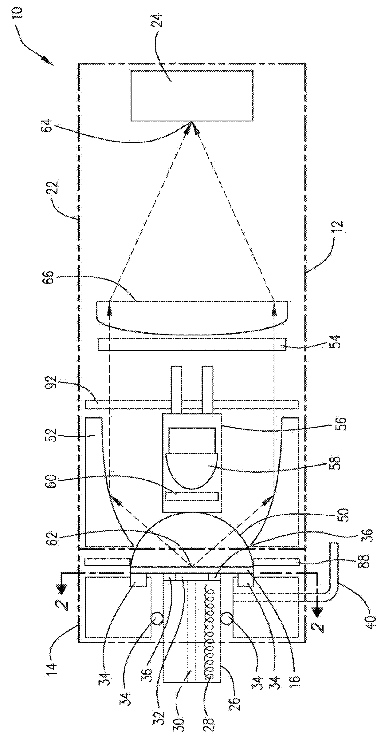
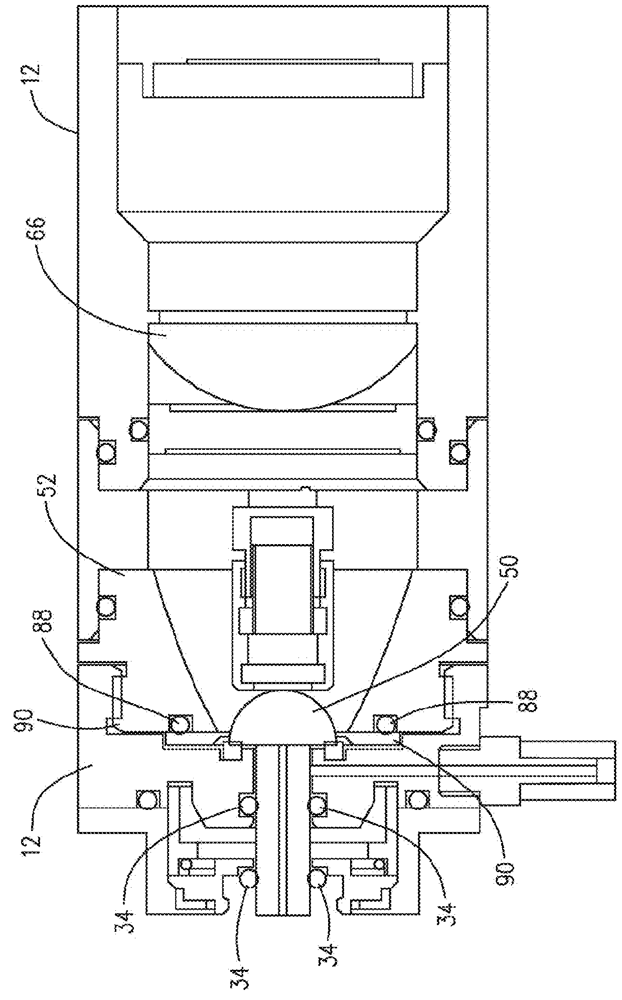
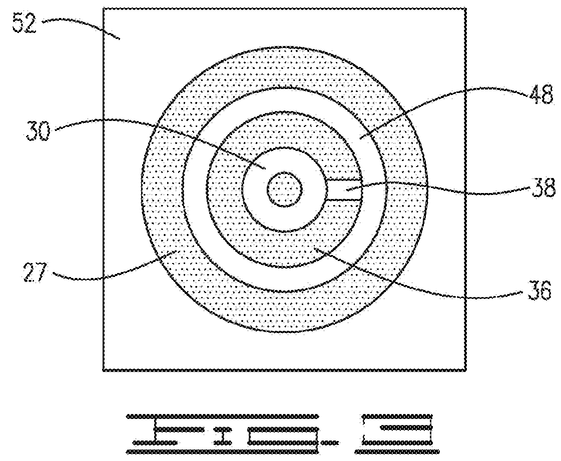
[0107]This invention provides for an apparatus to optically collect and detect changes in a fluorescing emission resulting from the reaction of an explosive, chemical or biological warfare substance with a reporter material such as a chemical warfare indicating chromophore (CWIC) or amplifying fluorescence polymer (AFP) material. The apparatus comprises three main elements: an air-sampling nozzle, fluorescence collection optics, and a detector / sensor.

I. SPCE Overview

[0108]Surface plasmon resonator (SPR) sensors are frequently used as surface binding detection techniques in chemical and biological material sensing applications. Due to the presence of an SPR-capable metal surface, an emission from a CWIC or AFP is coupled into the surface plasmon wave (SPW) and then re-radiated as SPCE via the surface plasmon coupled emission phenomenon. The SPW is a surface-bonded electromagnetic wave propagation in which the free electrons in a conductor, such as coated thin films of noble metals, c...


PUM

PropertyMeasurementUnit
half angleaaaaaaaaaa
heightaaaaaaaaaa
heightaaaaaaaaaa

Abstract

This invention generally relates to optical devices that can collect and detect signal emissions effectively while allowing the excitation light path and the sample flow path to coexist non-obstructively in a compact format. The device has various embodiments, such as an embodiment including a plurality of reporters disposed on a sensing surface, wherein each one of the plurality of reporters is configured to react with a least one target analyte, a hyperspectral detection module configured to capture hyperspectral image data corresponding to the plurality of reporters, and a controller. The controller is configured to receive the hyperspectral image data from the hyperspectral detection module and generate a temporal spectral signature corresponding to each one of the plurality of reporters from the received hyperspectral image data.

Description

CROSS-REFERENCE TO RELATED APPLICATIONS[0001]This application is a continuation-in-part of U.S. patent application Ser. No. 13 / 767,509, filed Feb. 14, 2013, which claims the benefit of U.S. Provisional Application No. 61 / 600,203, filed Feb. 17, 2012, and U.S. Provisional Application No. 61 / 614,228, filed Mar. 22, 2012, all three of which are hereby incorporated by reference herein.STATEMENT AS TO FEDERALLY SPONSORED RESEARCH[0002]This application was supported in part by a contract from the U.S. Army, Contract Number: W909MY-10-C-0037. The United States Government may have rights in, and to, this application by virtue of this funding.BACKGROUND[0003]The present invention is for a new inventive device and method to collect and detect optical fluorescent emissions from a reporter and an analyte. In particular, the present invention is an optical collection device for collecting fluorescent optical emissions at the molecular level, and a method for using the same. The molecular-based o...

Claims


Application Information

Patent Timeline
Patent Type & Authority Applications(United States)
IPC IPC(8): G01N21/64G01N33/22
CPCG01N21/648G01N33/227G01N2021/6423G01N21/643G01N21/6486G01N21/6428G01N21/645
Inventor JA, SHIOU-JYH
Owner FLIR DETECTION
Why Eureka
Try Eureka