Cleaning agent for metal wiring substrate, and method for cleaning semiconductor substrate

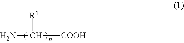
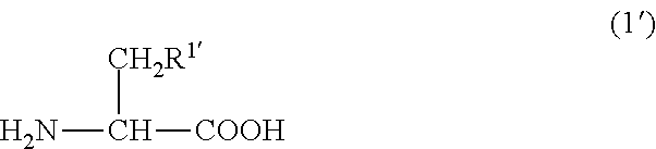
a cleaning agent and metal wiring technology, applied in the direction of electrical equipment, chemical instruments and processes, detergent compositions, etc., can solve the problems of increasing the resistance of the metal wiring, affecting the reliability of the semiconductor device, and inducing short-circuiting between the wirings, so as to achieve stable for a long time, without impairing the flatness of the metal wiring surface, and the effect of hard deterioration

Inactive Publication Date: 2016-03-03
WAKO PURE CHEMICAL INDUSTRIES
View PDF1 Cites 8 Cited by
  • Summary
  • Abstract
  • Description
  • Claims
  • Application Information

AI Technical Summary

Benefits of technology

[0022]The cleaning agent for the substrate having the metal wiring of the present invention is, in a manufacturing process of a semiconductor device, a cleaning agent to be used in a cleaning process for a semiconductor substrate after CMP process and a cleaning agent to be used preferably for a semiconductor substrate having, in particular, a copper wiring or a copper alloy wiring, and a cleaning agent exerting following effects (1) to (5). (1) Residues of fine particles (polishing agents) used in the CMP process, fine particles (metal particles) derived from a polished metal, an anticorrosive, and the like, can be removed sufficiently. (2) A coating film (protective film: oxidation resistant film) on the surface of the metal wiring, containing a complex between an anticorrosive, such as benzotriazole or quinaldic acid, and a surface metal of the metal wiring, formed in the CMP process, can be removed (stripped) sufficiently. (3) An oxide film containing a metal oxide can be formed after removal (stripping) of the coating film. (4) A semiconductor substrate can be obtained stably for a long period of time, without impairing flatness of the surface of the metal wiring (the surface of the oxide film containing the metal oxide), even leaving a substrate after the cleaning process after the CMP. (5) It is hard to deteriorate even after using the cleaning agent for a long period of time.
[0023]In addition, the cleaning method for the semiconductor substrate of the present invention is an effective method for cleaning the semiconductor substrate having the metal wiring, for example, a copper wiring, or the like, and by using the cleaning agent for the substrate having the metal wiring of the present invention. the semiconductor substrate can clean effectively and stably.
[0024]The present inventors have intensively studied a way to attain the above-described objects and found that only the cleaning agent, containing in combination of the carboxylic acid having the nitrogen-containing heterocyclic ring, among various carboxylic acids, and the alkylhydroxylamine, where a pH is adjusted to 10 or higher, can provide all of the above-described effects (1) to (5), and have thus completed the present invention.

Problems solved by technology

Such residues adversely affect electric characteristics of the semiconductor, such as short-circuiting between wirings, and resulting in decrease in reliability of the semiconductor device.
On the other hand, the metal wiring to be used in the manufacturing process of such a semiconductor device has high conductivity, as well as high metallic activity, and is thus easily oxidized (corroded) by external environment There has been a problem of increasing resistance of the metal wiring, or inducing short-circuiting between the wirings, due to such oxidation (corrosion).
In addition, there is the case of increasing resistance of the metal wiring, or inducing short-circuiting between the wirings, caused by generation of the polishing residue, scratching or dishing of the metal wiring, in the CMP process.
On the other hand, in a recent manufacturing process of a semiconductor device, there may be the case where waiting time of a substrate at the end of the cleaning process after the CMP is long, because the substrate finished the cleaning process after the CMP requires time till going forward to the next process such as a lamination process of the metal wiring, due to complicated manufacturing process caused by miniaturization of metal wiring.
In addition, in the case where the manufacturing process is stopped for a long period of time caused by troubles of manufacturing equipment, there has been increasing the situation where the substrate waits in the midst of the processes.

Method used


Image

  • Cleaning agent for metal wiring substrate, and method for cleaning semiconductor substrate
  • Cleaning agent for metal wiring substrate, and method for cleaning semiconductor substrate
  • Cleaning agent for metal wiring substrate, and method for cleaning semiconductor substrate

Examples


examples

[0064]Explanation on the present invention will be given specifically below based on Examples and Comparative Examples, however, the present invention should not be limited to these Examples. It should be noted that “%” in the following Examples and Comparative Examples is weight base (w / w %) unless specified in particular.

—Preparation Method of Substrate A for the Evaluation—

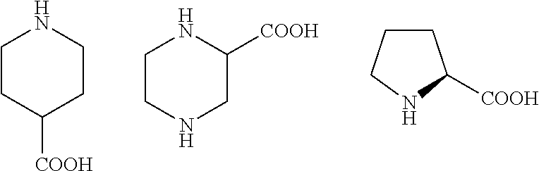
[0065]A wafer was purchased, wherein a surface of SEMATECH 845 (copper wiring, barrier metal: TaN, oxide film: TEOS; manufactured by SEMATECH Co., Ltd.), having a diameter of 8 inch, was polished with polishing slurry containing benzotriazole (BTA), and planarized, and then cleaned with pure water. The wafer was immersed in a 1% benzotriazole (BTA) aqueous solution for 1 hour, and a copper(I)-benzotriazole coating film was formed on the surface of the copper wiring, followed by rinsing with pure water using a single wafer processing cleaning machine (multi-spinner; manufactured by Kaijo Corp.), and spin-drying....


PUM

PropertyMeasurementUnit
pHaaaaaaaaaa
pHaaaaaaaaaa
weight %aaaaaaaaaa

Abstract

It is a subject of the present invention to provide a cleaning agent for a substrate having a metal wiring, and a cleaning method for a semiconductor substrate comprising that the cleaning agent is used, by which following effects (1) to (5) are obtained, in a cleaning process after chemical mechanical polishing (CMP) in a manufacturing process of a semiconductor device. (1) Residues of fine particles (polishing agents) used in the CMP process, fine particles (metal particles) derived from a polished metal, an anticorrosive, and the like, can be removed sufficiently. (2) A coating film (protective film: oxidation resistant film) on a surface of the metal wiring, containing a complex between an anticorrosive, such as benzotriazole or quinaldic acid, and a surface metal of the metal wiring, formed in the CMP process, can be removed (stripped) sufficiently. (3) An oxide film containing a metal oxide can be formed after removal (stripping) of the coating film. (4) A semiconductor substrate can be obtained stably for a long period of time, without impairing flatness of the surface of the metal wiring (the surface of the oxide film containing the metal oxide), even leaving a substrate after the cleaning process after the CMP. (5) It is hard to deteriorate even after using the cleaning agent for a long period of time.The present invention relates to a cleaning agent for a substrate having a metal wiring, comprising an aqueous solution containing (A) carboxylic acid having a nitrogen-containing heterocyclic ring and (B) alkylhydroxylamine, and having a pH of 10 or higher, as well as a cleaning method for a semiconductor substrate, comprising that the cleaning agent is used.

Description

TECHNICAL FIELD[0001]The present invention relates to a cleaning agent for a substrate having a metal wiring, and a cleaning method for a semiconductor substrate comprising that the cleaning agent is used. In more details, the present invention relates to a cleaning agent for a substrate having a metal wiring, to be used in a process for cleaning a semiconductor substrate after a chemical mechanical polishing (CMP) process, in a manufacturing process of a semiconductor device typified by a silicon semiconductor, and a cleaning method for a semiconductor substrate comprising that the cleaning agent is used.BACKGROUND ART[0002]In a semiconductor device typified by a silicon semiconductor or the like, a miniaturization and a high integration have been progressing, in compliance with market needs, such as higher performance, more compact sizing. Along with the miniaturization and the high integration, such a semiconductor substrate has been required that have a metal wiring having high ...

Claims


Application Information

Patent Timeline
Patent Type & Authority Applications(United States)
IPC IPC(8): C11D11/00C11D7/32H01L21/02
CPCC11D11/0047H01L21/02074C11D7/3218C11D7/3281C11D7/3209
Inventor MIZUTA, HIRONORIWATAHIKI, TSUTOMUMAESAWA, TSUNEAKI
Owner WAKO PURE CHEMICAL INDUSTRIES
Why Eureka
Try Eureka