Photoelectric Conversion Element, Photoelectric Conversion Element Having Storage/Discharge Function, and Secondary Battery

a technology of photoelectric conversion and storage/discharge function, which is applied in the direction of solid-state devices, climate sustainability, flat cell grouping, etc., can solve the problems of inability to carry out power generation, limited weight reduction, and extremely difficult imparting flexibility, etc., and achieve stably supply power and efficient operation.

Inactive Publication Date: 2016-03-10
SELMO ENTERTAINMENT JAPAN
View PDF0 Cites 10 Cited by
  • Summary
  • Abstract
  • Description
  • Claims
  • Application Information

AI Technical Summary

Benefits of technology

[0064]The photoelectric conversion element of the present invention contains a fullerene, a conductive polymer and an organic pigment in the n-type compound semiconductor layer, and when the photoelectric conversion element is irradiated with visible light or infrared light, the light is absorbed by the organic pigment to excite the organic pigment, and charge separation occurs in the conductive polymer. This charge separation state is taken over to the fullerene that is connected to the conductive polymer, and the excited minus charge is accumulated in the substrate layer that is a minus electrode, through the collector electrode, while positive holes generated in the p-type compound semiconductor layer are accumulated in the plus electrode 22 through the conductive metal 26, whereby a potential difference is produced between the plus electrode 22 and the substrate layer 12 that is a minus electrode. Therefore, by virtue of irradiation with light, the photoelectric conversion element 10 shown in FIG. 1 functions as a solar battery.
[0065]The photoelectric conversion element having storage/discharge ability of the present invention roughly has constitution wherein such a photoelectric conversion element as above and a secondary battery are united. Owing to minus charge produced by driving of the photoelectric conversion element, the secondary battery minus electrode face 42 of the storage battery arranged on the back surface of the substrate layer 12 and the ferroelectric layer 44 are negatively charged, and parting by the solid electrolyte layer, the second electrolyte layer 48 and the secondary battery plus electrode face 50 are positively charged. As a result, power generated in the photoelectric conversion element of the present invention is stored in the secondary battery arranged on the back surface. On the other hand, when the photoelectric conversion element of the present invention cannot generate power in the nighttime or th...

Problems solved by technology

In the photoelectric conversion elements, however, there are various problems such that power generation cannot be carried out in the nighttime of no sunlight irradiation, the power generation quantity varies depending upon the weather, weight reduction is limited because silicon wafer is generally used as an electrode, impartation of flexibility is extremely difficult because silicon wafer is used, and ...

Method used


Image

  • Photoelectric Conversion Element, Photoelectric Conversion Element Having Storage/Discharge Function, and Secondary Battery
  • Photoelectric Conversion Element, Photoelectric Conversion Element Having Storage/Discharge Function, and Secondary Battery
  • Photoelectric Conversion Element, Photoelectric Conversion Element Having Storage/Discharge Function, and Secondary Battery

Examples


example 1

First Step

[0323]In an Erlenmeyer flask having a volume of 300 ml, 50 ml of toluene (C6H5CH3, molecular weight: 92.14) was placed, and 22.2 g of di-2-ethylhexyl sodium sulfosuccinate (C20H37NaO7S, molecular weight: 444.56) was placed therein. The flask was sealed with a rubber stopper to block the outside air, and the contents in the flask were stirred for 10 minutes to completely dissolve di-n-ethylhexyl sodium sulfosuccinate in toluene.

Second Step

[0324]To the toluene solution obtained in the first step, 20 ml of aniline (C6H7N, molecular weight: 93.13) was added, and they were stirred for 5 minutes until the mixture became a homogeneous light yellow solution.

Third Step

[0325]To 180 ml of pure water (H2O) was added 20 ml of hydrochloric acid (37% aqueous solution of HCl) to prepare 200 ml of a hydrochloric acid aqueous solution. While stirring the light yellow solution obtained in the second step by a magnetic stirrer, 150 ml of the above-prepared hydrochloric acid aqueous solution w...

example 2

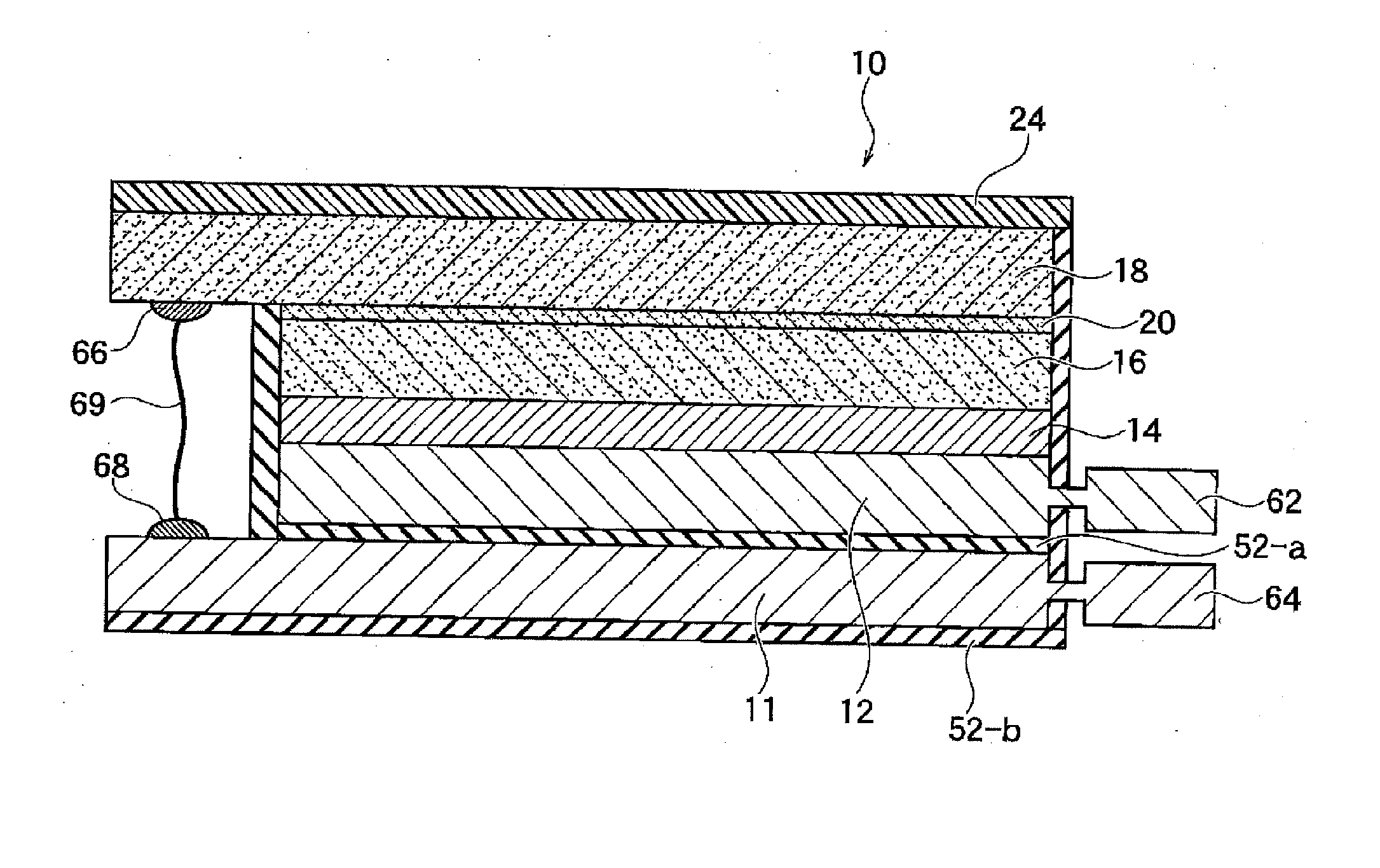
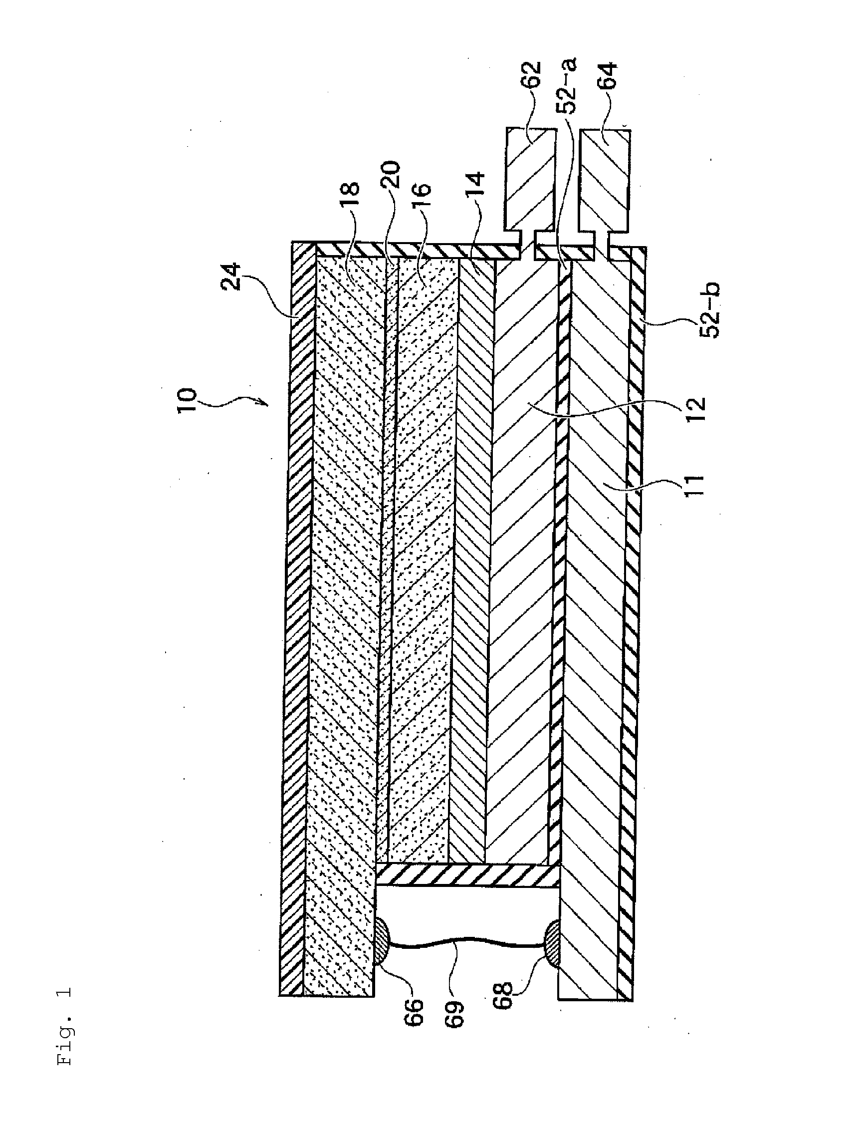
[0379]Example of production of storage element (secondary battery) in which layer of ferroelectric substance (strontium titanate or the like) coated with ion adsorption substance such as graphene and layer of ion supply substance (e.g., alkali metal salt bonded to graphene) are arranged interposing therebetween solid electrolyte such as vanadate and which utilizes adsorption of ion molecule and charge accumulation of ferroelectric

[0380]Step i

[0381]A quartz cover glass of 18 mm×18 mm was used as a substrate 86, and on the whole surface of the substrate 86, sputtering was carried out using pure copper as a target to form a sputtered film having a thickness of 100 nm to 500 nm. This sputtered film (copper) becomes a collector electrode (copper) 85 and also becomes an electrode.

[0382]Step ii

[0383]On a surface of the copper sputtered film formed in the step i, a heat-resistant polyimide tape was applied in such a manner that an opening of 5 mm×5 mm was formed, whereby masking was carried...

example 3

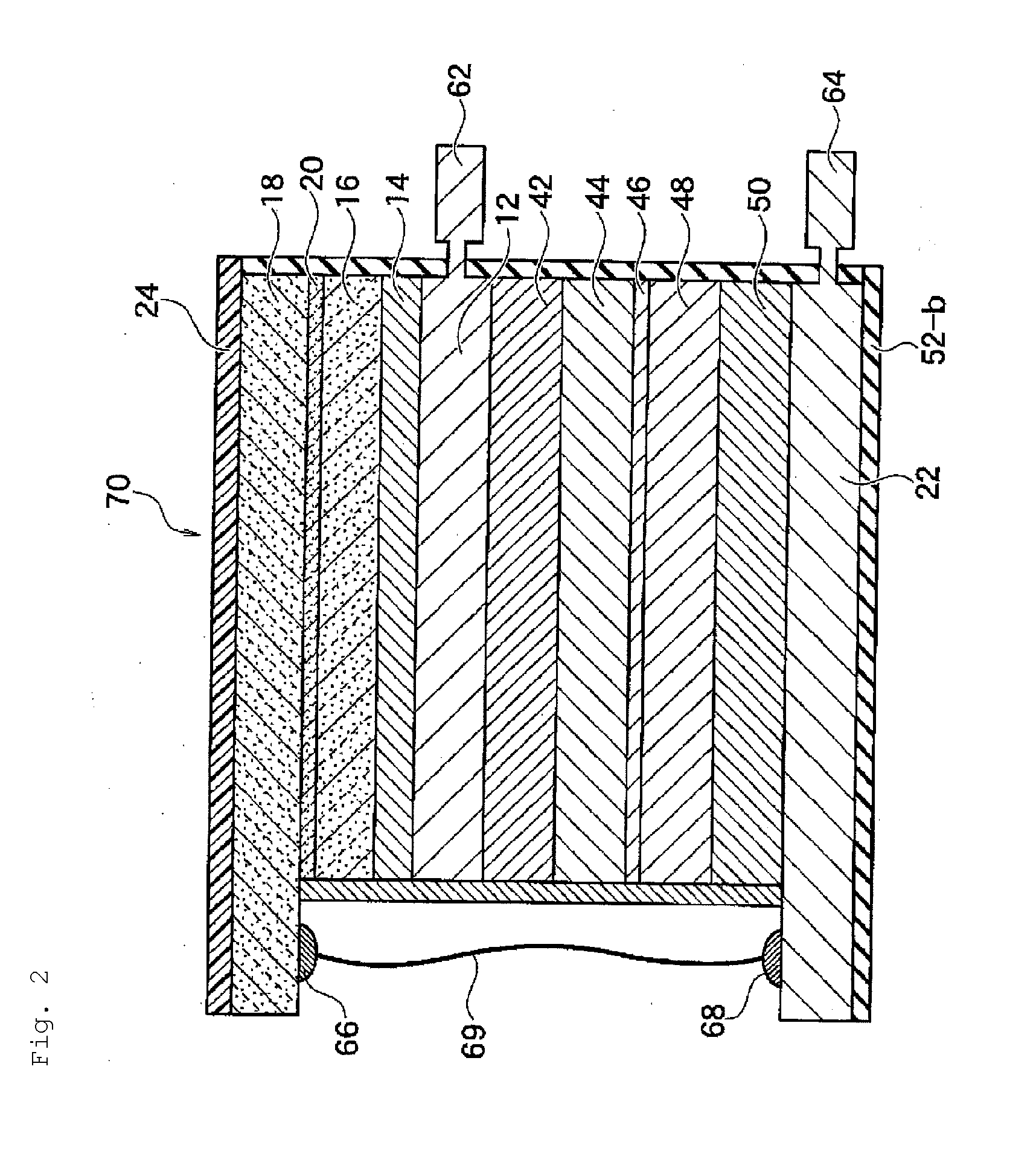
[0407]Example of photoelectric conversion element having storage effect in which power generation layer and power storage layer are combined as shown in FIG. 13

[0408]Step a

[0409]A quartz cover glass of 18 mm×18 mm was used as a substrate 98, and on the whole surface of the substrate 98, sputtering was carried out using pure copper as a target to form a sputtered film having a thickness of 100 nm to 500 nm. This sputtered film (copper) becomes a collector electrode (copper) 97 and also becomes an electrode.

[0410]Step b

[0411]On a surface of the copper sputtered film formed in the step a, a heat-resistant polyimide tape was applied in such a manner that an opening of 5 mm×5 mm was formed, whereby masking was carried out.

[0412]Step c

[0413]The substrate obtained in the step (b) was heated to 100 to 150° C., and a p-type organic semiconductor was casted to form a film. The thickness of this p-type organic semiconductor layer 96 was 100 to 500 nm.

[0414]Step d

[0415]A pn-bulk layer material ...


PUM

PropertyMeasurementUnit
Temperatureaaaaaaaaaa
Electric potential / voltageaaaaaaaaaa
Metallic bondaaaaaaaaaa

Abstract

A photoelectric conversion element having storage/discharge ability has a substrate layer that is formed of a conductive metal and is connected to a minus electrode of output electrodes, a collector electrode that is formed by being joined to one surface of the substrate layer, an n-type compound semiconductor layer that is formed of a dielectric composition containing a fullerene and is formed by being connected to the collector electrode, a p-type compound semiconductor layer that is formed in contact with the n-type compound semiconductor layer, and a pn-bulk layer that is formed between the n-type compound semiconductor layer and the p-type compound semiconductor layer and is intermittently in contact with the n-type compound semiconductor layer and the p-type compound semiconductor layer, and has a secondary battery arranged on the other surface of the substrate layer to provide a storage/discharge function. Also provided is the secondary battery preferably used herein.

Description

TECHNICAL FIELD[0001]The present invention relates to a photoelectric conversion element utilizing fullerenes, a photoelectric conversion element having a storage / discharge function and a secondary battery which can be preferably used for the photoelectric conversion element utilizing fullerenes.BACKGROUND ART[0002]With changes of energy sources, photoelectric conversion elements (solar batteries) have been recently noted. The photoelectric conversion elements have various advantages such that they have no drive part and rarely break down because they produce electrical energy directly from sunlight, and there is no limitation on the installation location provided that it is a place in the light. Therefore, instances in which the photoelectric conversion elements are installed on the roofs of individual houses or on the rooftops of buildings are increasing.[0003]In the photoelectric conversion elements, however, there are various problems such that power generation cannot be carried...

Claims


Application Information

Patent Timeline
IPC IPC(8): H01L51/42H01L51/00H01M4/38H01M4/48H01M4/583H01M10/0565H01M10/0568H01M10/46H02S40/38
CPCH01M4/48H01M4/583H01M10/0568H01M10/0565H01M10/46H02S40/38H01L51/0046H01L51/4293H01L51/0048H01L51/4213H01L51/0036H01L51/0035H01L51/0078H01L51/0097H01L51/0047H01M4/38H01G9/2013H01G9/2059H01M4/483H01M4/663H01M10/052H01M10/054H01M10/056H01M10/0585H01M10/465H01M2300/0088H01M2300/0094Y02E10/549Y02E60/10Y02E70/30H10K85/215H10K85/621H10K85/655H10K85/30H10K85/371H10K30/00H10K85/211H10K30/10H10K30/40H10K77/111H10K85/111H10K85/113H10K85/221H10K85/311
Inventor YUMURA, SHINICHIRO
Owner SELMO ENTERTAINMENT JAPAN
Why Eureka
Try Eureka