Switching power supply device, and inverter, converter, and solar power controller including same

a technology of switching power supply and inverter, which is applied in the direction of pulse technique, process and machine control, instruments, etc., can solve the problems of large switching loss and high cos

Active Publication Date: 2016-06-02
SHARP KK
View PDF8 Cites 8 Cited by
  • Summary
  • Abstract
  • Description
  • Claims
  • Application Information

AI Technical Summary

Benefits of technology

[0008]According to a preferred embodiment of the present invention, in a second transistor having a low withstand voltage compared to a first transistor having a high withstand voltage, a recovery current caused by a built-in diode is small. Subsequently, when current flows from a second node to a first node, the first transistor turns on and the second transistor turns off, and thus a current flows only to the built-in diode of the second transistor having a small recovery current, without a current flowing to the built-in diode of the first transistor having a large recovery current. Consequently, the built-in diodes of the transistors preferably are utilized without externally attaching a freewheeling diode, and losses due to recovery current are reduced. As a result, a highly efficient and low-cost switching power supply device is provided.
[0009]Also, according to a preferred embodiment of the present invention, the first transistor having a high withstand voltage and the second transistor having a low withstand voltage are connected in series, and the second transistor having a low withstand voltage performs the switching operation. Since the majority of the power supply voltage is applied between a first electrode and a second electrode of the first transistor having a high withstand voltage, the voltage between a first electrode and a second electrode of the second transistor having a low withstand voltage that performs the switching operation is able to be small. For this reason, the degree of influence on the electric potential of the control electrode of the second transistor that performs the switching operation exerted due to variation in the electric potential of the capacitively coupled first electrode is able to be small. As a result, misfiring of the second transistor due to variation in the electric potential of the control electrode is effectively reduced or prevented. Consequently, a highly reliable switching power supply device is provided.
[0010]Also, according to a preferred embodiment of the present invention, in at least one of either the first or the second transistor, it is possible to decide independently the speeds at which the electric potential of the control electrode increases and decreases. Consequently, since the rising and falling speeds of switching is able to be decided independently, more precise switching of the circuit is able to be sped up within a range in which the circuit does not oscillate, and losses are significantly reduced or eliminated.

Problems solved by technology

In such cases, if a power supply voltage is applied in the reverse direction to the parasitic diode while an electrical current is flowing back in the forward direction to the parasitic diode, recovery current (reverse recovery current) flows to the parasitic diode, generating a large switching loss.
However, there is a problem with the method of Japanese Unexamined Patent Application Publication No.
There is also a problem with the method of Japanese Unexamined Patent Application Publication No. 2010-29019, in that costs become high as a result of providing two MOS transistors and a freewheeling diode having a high withstand voltage.

Method used


Image

  • Switching power supply device, and inverter, converter, and solar power controller including same
  • Switching power supply device, and inverter, converter, and solar power controller including same
  • Switching power supply device, and inverter, converter, and solar power controller including same

Examples


first preferred embodiment

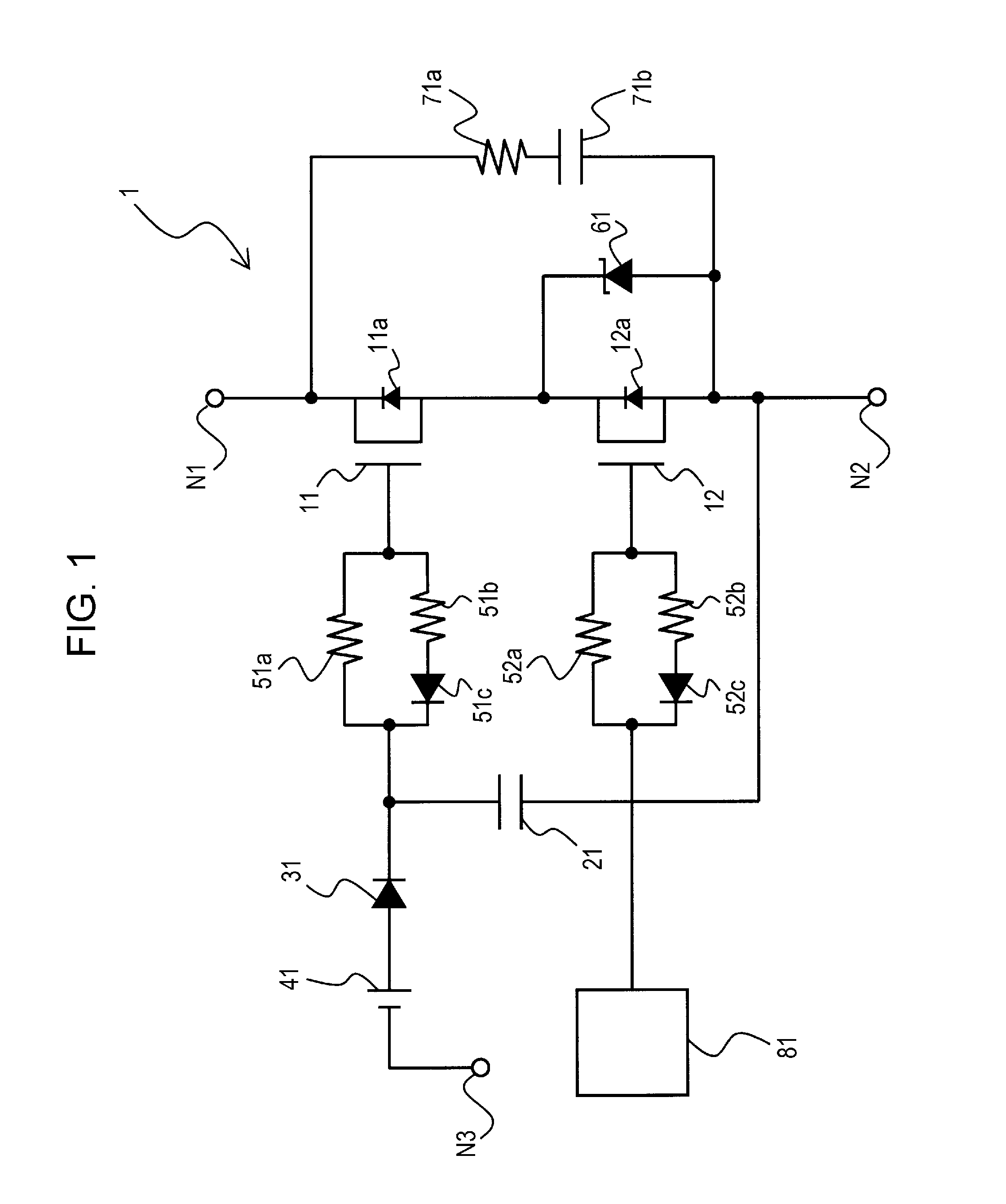
[0020]As illustrated in FIG. 1, a switching power supply device 1 according to a first preferred embodiment of the present invention includes n-channel MOS transistors 11 and 12, capacitors 21 and 71b, diodes 31, 51c, and 52c, a gate power supply 41, resistors 51a, 51b, 52a, 52b, and 71a, a Zener diode 61, and a gate driver 81. The transistors 11 and 12 have built-in parasitic diodes 11a and 12a, respectively.

[0021]An anode of each of the parasitic diodes 11a and 12a is connected to a source (second electrode) of the corresponding transistor 11 (first transistor) and transistor 12 (second transistor), respectively, while a cathode of each of the parasitic diodes 11a and 12a is connected to a drain (first electrode) of the corresponding transistors 11 and 12, respectively.

[0022]The transistor 11 is a high withstand voltage transistor, having a source-drain withstand voltage of 600 V, for example. The transistor 12 is a low withstand voltage transistor, having a source-drain withstand...

second preferred embodiment

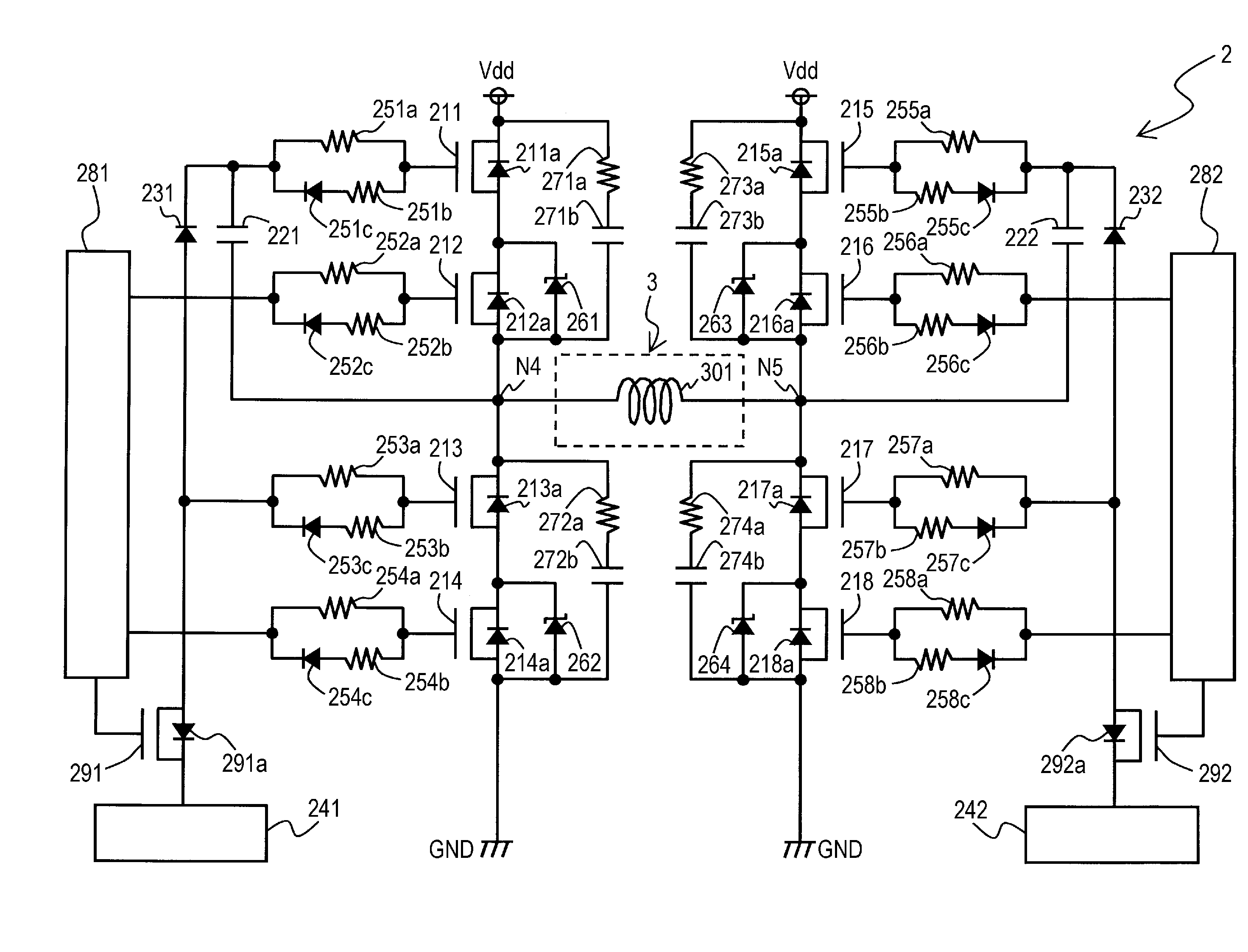
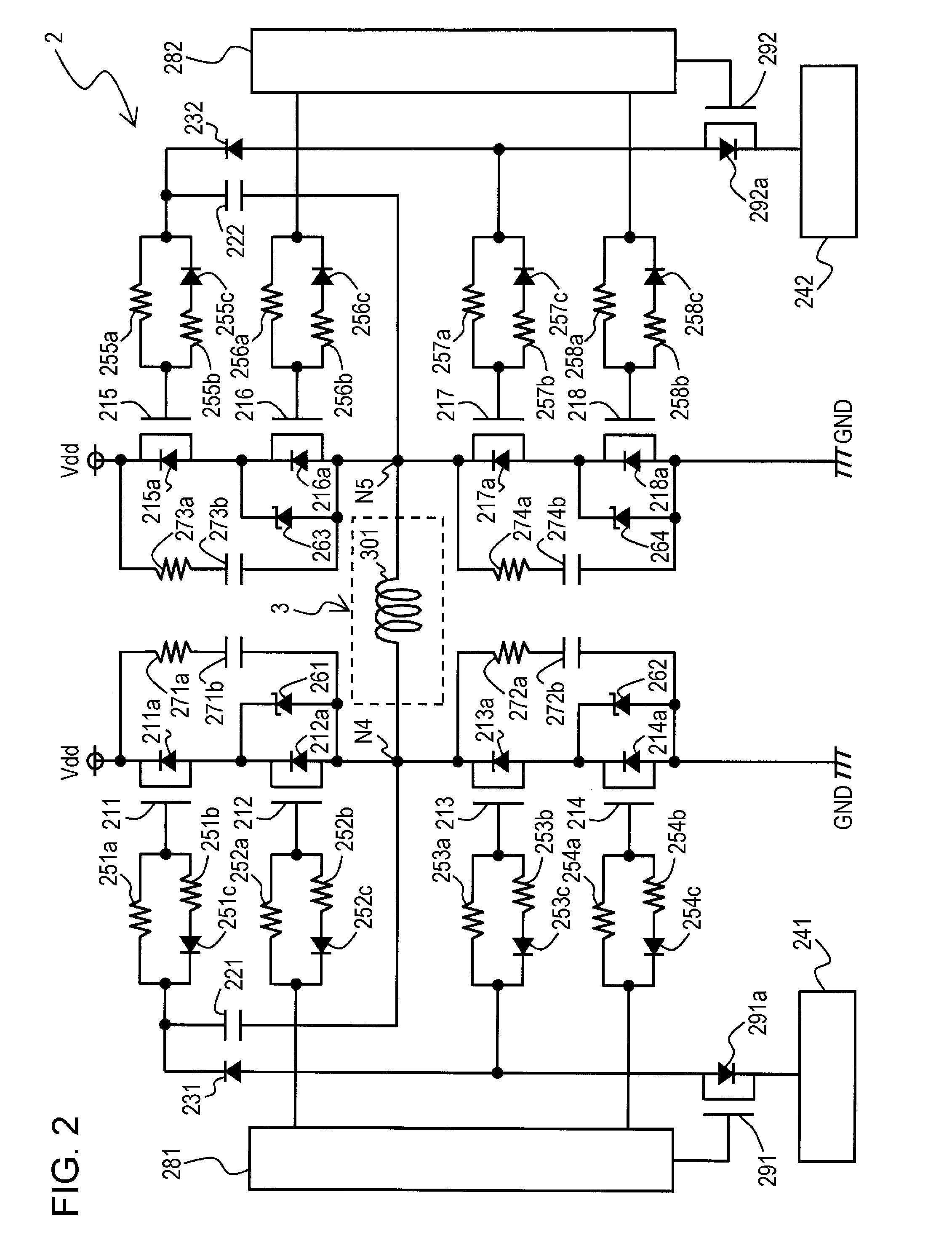
[0081]As illustrated in FIG. 2, an inverter 2 according to a second preferred embodiment of the present invention includes n-channel MOS transistors 211 to 218, 291, and 292, capacitors 221, 222, and 271b to 274b, diodes 231, 232, and 251c to 258c, gate power supplies 241 and 242, resistors 251a to 258a, 251b to 258b, and 271a to 274a, Zener diodes 261 to 264, and gate drivers 281 and 282. The transistors 211 to 218, 291, and 292 have built-in parasitic diodes 211a to 218a, 291a, and 292a, respectively.

[0082]An anode of each of the parasitic diodes 211a to 218a, 291a, and 292a is connected to a source of each of the corresponding transistors 211 to 218, 291, and 292, respectively, while a cathode of each of a parasitic diodes 211a to 218a, 291a, and 292a is connected to a drain of each of the corresponding transistors 211 to 218, 291, and 292, respectively.

[0083]Each of the transistors 211, 213, 215, and 217 is a high withstand voltage transistor, having a source-drain withstand vol...

third preferred embodiment

[0122]FIG. 5 illustrates a step-up chopper 4 according to a third preferred embodiment of the present invention. The step-up chopper 4 includes a circuit that is similar to the inverter 2. The step-up chopper 4 and the inverter 2 are different only in that the upper-left and lower-left arms and the upper-right and lower-right arms are joined by a coil 401 which is part of the step-up chopper 4, the drain of the transistor 215 of the upper-right arm is connected to an input terminal Vin, and the drain of the transistor 211 of the upper-left arm is connected to an output terminal Vout. Note that description will be reduced or omitted for elements having the same reference numerals as the inverter 2.

[0123]Operation of the step-up chopper will be described. When the transistors 214 and 216 are turned on, current flows from the input terminal Vin, through the transistors 215 and 216, the coil 401, and the transistors 213 and 214, to the ground voltage GND line, and electromagnetic energy...


PUM


Abstract

A highly efficient and low-cost switching power supply device includes a high withstand voltage transistor and a low withstand voltage transistor. When current flows from a second node to a first node, the high withstand voltage transistor turns on and the low withstand voltage transistor turns off, causing current to flow through a built-in diode of the low withstand voltage transistor. Since current does not flow through the parasitic diode of the high withstand voltage transistor, the recovery current is reduced. Furthermore, since a first delay circuit including resistors and a diode is connected to the gate electrode of the high withstand voltage transistor, and a second delay circuit including resistors and a diode is connected to the gate electrode of the low withstand voltage transistor, precise adjustment of the switching speed during switching operation is possible, and losses are reduced.

Description

TECHNICAL FIELD[0001]The present invention relates to a switching power supply device, and more particularly, to a switching power supply device with low switching loss, and to an inverter, a converter, and a solar power controller including the same.BACKGROUND ART[0002]In the past, there have been cases in which a metal-oxide-semiconductor (MOS) transistor parasitic diode is used as a freewheeling diode in an inverter. In such cases, if a power supply voltage is applied in the reverse direction to the parasitic diode while an electrical current is flowing back in the forward direction to the parasitic diode, recovery current (reverse recovery current) flows to the parasitic diode, generating a large switching loss.[0003]Japanese Unexamined Patent Application Publication No. H7-264876 discloses a method of preventing flow of recovery current by connecting a backflow prevention diode in the forward direction between a node on the high-voltage side and the drain of the MOS transistor,...

Claims


Application Information

Patent Timeline
Patent Type & Authority Applications(United States)
IPC IPC(8): H02M3/158H02M7/44
CPCH02M7/44H02M3/158H02M1/08H02M7/5387H03K17/163H03K17/6871H03K2217/0036H03K17/74H02J2300/24H02J3/381Y02B70/10Y02E10/56H02M1/0054
Inventor SHIBATA, AKIHIDEWAKAIKI, SHUJIKATAOKA, KOHTAROHSHIOMI, TAKESHIIGARASHI, HIROKIIWATA, HIROSHI
Owner SHARP KK
Why Eureka
Try Eureka