NVMM: An Extremely Large, Logically Unified, Sequentially Consistent Main-Memory System

a main-memory system, logically unified technology, applied in the direction of memory architecture accessing/allocation, memory adressing/allocation/relocation, instruments, etc., can solve the problems of large problems, the entire system runs at the speed of the slowest component, and the high-level cache becomes useless. , to achieve the effect of large solid-state capacity

Inactive Publication Date: 2016-09-01
JACOB BRUCE LEDLEY
View PDF4 Cites 23 Cited by
  • Summary
  • Abstract
  • Description
  • Claims
  • Application Information

AI Technical Summary

Benefits of technology

[0009]Embodiments of the present invention provide a novel memory-system architecture and multi-node processing having a non-volatile flash main memory subsystem as the byte-addressable main memory, and cache volatile memory front-end for the flash subsystem. Disclosed embodiments reveal a memory-system architecture having many features desirable in modern large-scale computing centers like enterprise computing systems and supercomputers. Disclosed embodiments reveal an extremely large solid-state capacity (at least a terabyte of main memory per CPU socket); power dissipation lower than that of DRAM; cost-per-bit approaching that of NAND flash memory; and performance approaching that of pure DRAM—all in an overall non-volatile memory-system architecture.

Problems solved by technology

Memory systems for large datacenters, such as telecommunications, cloud providers, enterprise computing systems, and supercomputers, are all based on memory architectures derived from the same 1970s era dynamic random access memory (DRAM) organization, and suffer from significant problems because of that DRAM-based memory architecture.
These memory systems were never designed, or optimized, to handle the requirements now placed on them: they do not provide high per-socket capacity, except at extremely high price points; they dissipate significant power, on par with the processing components; they are not sequentially consistent and rely upon the processor network to provide both consistency and coherence; and these large data centers are huge, having millions of semiconductor parts, and therefore single device failures are common, requiring the practice of checkpointing, saving a snapshot of the application's state, so that it can restart from that saved state in case of failure.
In these systems, the main memory system was designed to lie at the bottom of the memory hierarchy, with its poor performance hidden by higher-level caches, and when extremely large data sets are streamed out of it, the high-level caches become useless, and the entire system runs at the speed of the slowest component.
Thus, tremendous bandwidth is needed to overcome this situation.
But DRAM is no longer the cheapest, the densest, nor the lowest-power storage technology available.
For both technical and economic reasons, it is no longer feasible to build ever-larger main memory systems out of DRAM.

Method used


Image

  • NVMM: An Extremely Large, Logically Unified, Sequentially Consistent Main-Memory System
  • NVMM: An Extremely Large, Logically Unified, Sequentially Consistent Main-Memory System
  • NVMM: An Extremely Large, Logically Unified, Sequentially Consistent Main-Memory System

Examples


Embodiment Construction

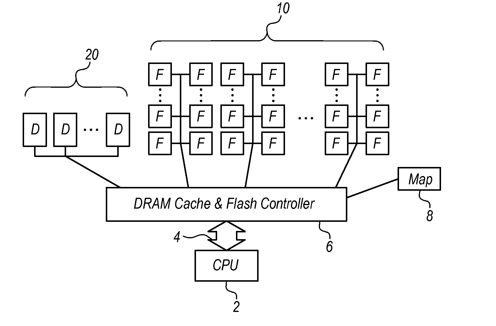
[0038]Revisiting the design choice of ever-larger main memory systems of DRAM, an obvious alternative is NAND flash. In one embodiment, a single node flash-centric memory system is disclosed.

[0039]The operating system's file system has traditionally accessed NAND flash memory because NAND flash is a slow, block-oriented device, and the software overheads of accessing it through the file system are small relative to the latency of retrieving data from the flash device. However, if flash were used for main memory, it would be accessed through a load / store interface, which is what main memory demands. For comparison, a file-system access requires a system call to the operating system, a potential context switch, and layers of administrative operations in the operating system—all of which add up to thousands of instructions of overhead; on the other hand, a load / store interface requires but a single instruction: a load or store, which directly reads or writes the main memory, often by w...


PUM


Abstract

Embodiments of both a non-volatile main memory (NVMM) single node and a multi-node computing system are disclosed. One embodiment of the NVMM single node system has a cache subsystem composed of all DRAM, a large main memory subsystem of all NAND flash, and provides different address-mapping policies for each software application. The NVMM memory controller provides high, sustained bandwidths for client processor requests, by managing the DRAM cache as a large, highly banked system with multiple ranks and multiple DRAM channels, and large cache blocks to accommodate large NAND flash pages. Multi-node systems organize the NVMM single nodes in a large inter-connected cache/flash main memory low-latency network. The entire interconnected flash system exports a single address space to the client processors and, like a unified cache, the flash system is shared in a way that can be divided unevenly among its client processors: client processors that need more memory resources receive it at the expense of processors that need less storage. Multi-node systems have numerous configurations, from board-area networks, to multi-board networks, and all nodes are connected in various Moore graph topologies. Overall, the disclosed memory architecture dissipates less power per GB than traditional DRAM architectures, uses an extremely large solid-state capacity of a terabyte or more of main memory per CPU socket, with a cost-per-bit approaching that of NAND flash memory, and performance approaching that of an all DRAM system.

Description

CROSS-REFERENCES TO RELATED APPLICATIONS[0001]This non-provisional United States (U.S.) patent application claims the benefit of U.S. Provisional Patent Application No. 61 / 955,250 entitled NVMM: An Extremely Large, Logically Unified, Sequentially Consistent Main-Memory SystemFIELD OF THE INVENTION[0002]The present invention relates to computer memory, and more particularly to a new distributed, multi-node cache and main memory architecture.BACKGROUND OF THE INVENTION[0003]Memory systems for large datacenters, such as telecommunications, cloud providers, enterprise computing systems, and supercomputers, are all based on memory architectures derived from the same 1970s era dynamic random access memory (DRAM) organization, and suffer from significant problems because of that DRAM-based memory architecture. These memory systems were never designed, or optimized, to handle the requirements now placed on them: they do not provide high per-socket capacity, except at extremely high price po...

Claims


Application Information

Patent Timeline
Patent Type & Authority Applications(United States)
IPC IPC(8): G06F3/06G06F12/08
CPCG06F3/0679G06F12/0806G06F2212/62G06F3/0638G06F2212/7202G06F3/0604G06F12/0246G06F12/0873G06F12/1009G06F13/16G06F9/4401G11C29/82G06F2212/1016G06F2212/1032G06F2212/202G06F2212/282G06F2212/313G06F2212/7201G06F2212/7208G06F13/1694
Inventor JACOB, BRUCE LEDLEY
Owner JACOB BRUCE LEDLEY
Why Eureka
Try Eureka