Spin-orbit-torque magnetoresistive random access memory with voltage-controlled anisotropy

a random access memory and spin-orbit-torque technology, applied in the field of electrical devices, can solve the problems of poor read speed and write reliability, loss of stored information of volatile ram, and inability to perfect conventional mram devices, so as to and reduce the magnetic anisotropy of the free layer

Inactive Publication Date: 2016-09-15
QUALCOMM INC
View PDF2 Cites 24 Cited by
  • Summary
  • Abstract
  • Description
  • Claims
  • Application Information

AI Technical Summary

Benefits of technology

[0004]Magnetoresistive Random Access Memory (MRAM) is a non-volatile memory technology having response (read and write) times comparable to volatile memory. Data stored in MRAM does not degrade over time and, compared to other RAM technologies, MRAM uses very little power. In contrast with conventional RAM technologies, which store data as electric charges or current flows, MRAM uses magnetic storage elements. Thus, MRAM has several desirable characteristics that make it a candidate for a universal memory, such as high speed, high density (i.e., small bitcell size), low power consumption, and no logic state degradation over time.
[0009]Exemplary methods and apparatus for writing data to a three-terminal spin-orbit-torque magnetoresistive memory having a magnetoresistive tunnel junction (MTJ) including a free layer located between an oxide barrier layer and a substantially planar spin hall-effect material are provided. An exemplary method includes applying a first voltage across the MTJ to reduce a magnetic anisotropy of the free layer by inducing an electric field across the oxide barrier layer, as well as applying a second voltage across the substantially planar spin hall-effect material to cause a current to flow through the substantially planar spin hall-effect material and thereby apply a spin-orbit torque to the free layer, thus causing the free layer to switch between a parallel state and an antiparallel state. The electric field can be induced in a manner that reduces the magnetic anisotropy of the free layer from a naturally-occurring anisotropy of the free layer. The decreased magnetic anisotropy of the free layer can reduce a switching current of the MTJ.
[0011]In another example, provided is an apparatus including a memory controller configured to write data to a three-terminal spin-orbit-torque magnetoresistive memory having a magnetoresistive tunnel junction (MTJ) including a free layer located between an oxide barrier layer and a substantially planar spin hall-effect material. The memory controller can include means for applying a first voltage across the MTJ to reduce a magnetic anisotropy of the free layer by inducing an electric field across the oxide barrier layer, as well as means for applying a second voltage across the substantially planar spin hall-effect material to cause a current to flow through the substantially planar spin hall-effect material and thereby apply a spin-orbit torque to the free layer, thus causing the free layer to switch between a parallel state and an antiparallel state. The electric field can be induced in a manner that reduces the magnetic anisotropy of the free layer from a naturally-occurring anisotropy of the free layer. The reducing the magnetic anisotropy of the free layer can reduces a switching current of the MTJ. In an example, the means for applying the first voltage across the MTJ includes means for applying the voltage between the substantially planar spin hall-effect material and an MTJ electrode.
[0013]In another example, provided is an apparatus including a memory controller configured to write data to a three-terminal spin-orbit-torque magnetoresistive memory having a magnetoresistive tunnel junction (MTJ) including a free layer located between an oxide barrier layer and a substantially planar spin hall-effect material. The memory controller is configured to apply a first voltage across the MTJ to reduce a magnetic anisotropy of the free layer by inducing an electric field across the oxide barrier layer. The memory controller is also configured to apply a second voltage across the substantially planar spin hall-effect material to cause a current to flow through the substantially planar spin hall-effect material and thereby apply a spin-orbit torque to the free layer, thus causing the free layer to switch between a parallel state and an antiparallel state. The memory controller can be configured to induce the electric field in a manner that reduces the magnetic anisotropy of the free layer from a naturally-occurring anisotropy of the free layer. The reducing the magnetic anisotropy of the free layer can reduce a switching current of the MTJ. The memory controller can be configured to apply the first voltage across the MTJ between the substantially planar spin hall-effect material and an MTJ electrode.

Problems solved by technology

Volatile RAM loses its stored information whenever power is removed.
Despite the characteristics described above, conventional MRAM devices are not perfect.
The shared read and write paths create problems for read speed and write reliability.
However, a thin barrier layer is more susceptible to dielectric breakdown due to repeated write operations.
Also, a state of an MTJ can be flipped unintentionally by a read current.
This is called a “read disturbance.” As MTJ technology scales down in physical size, switching current tends to decrease.
However, high-speed read operations typically require more read current.
Therefore, high-speed MRAM, and particularly deeply-scaled MTJ devices, may suffer from a read disturbance.
Accordingly, it is challenging to meet reliability requirements for both write endurance (due to strain on a tunnel barrier in the MTJ) and read reliability.
Further, switching current asymmetry in conventional bottom-pinned two-terminal MTJ devices is incompatible with conventional N-type metal-oxide-semiconductor (NMOS) drive transistors.
Further, a driving power of a write transistor coupled in series with a conventional bottom-pinned two-terminal MTJ device also has asymmetry that is not compatible with writing Ic asymmetry of the conventional bottom-pinned two-terminal MTJ devices.
This leads to wasted energy during a write process, complicated MRAM and MTJ devices, read disturbances, and write endurance problems.

Method used


Image

  • Spin-orbit-torque magnetoresistive random access memory with voltage-controlled anisotropy
  • Spin-orbit-torque magnetoresistive random access memory with voltage-controlled anisotropy
  • Spin-orbit-torque magnetoresistive random access memory with voltage-controlled anisotropy

Examples


Embodiment Construction

Introduction

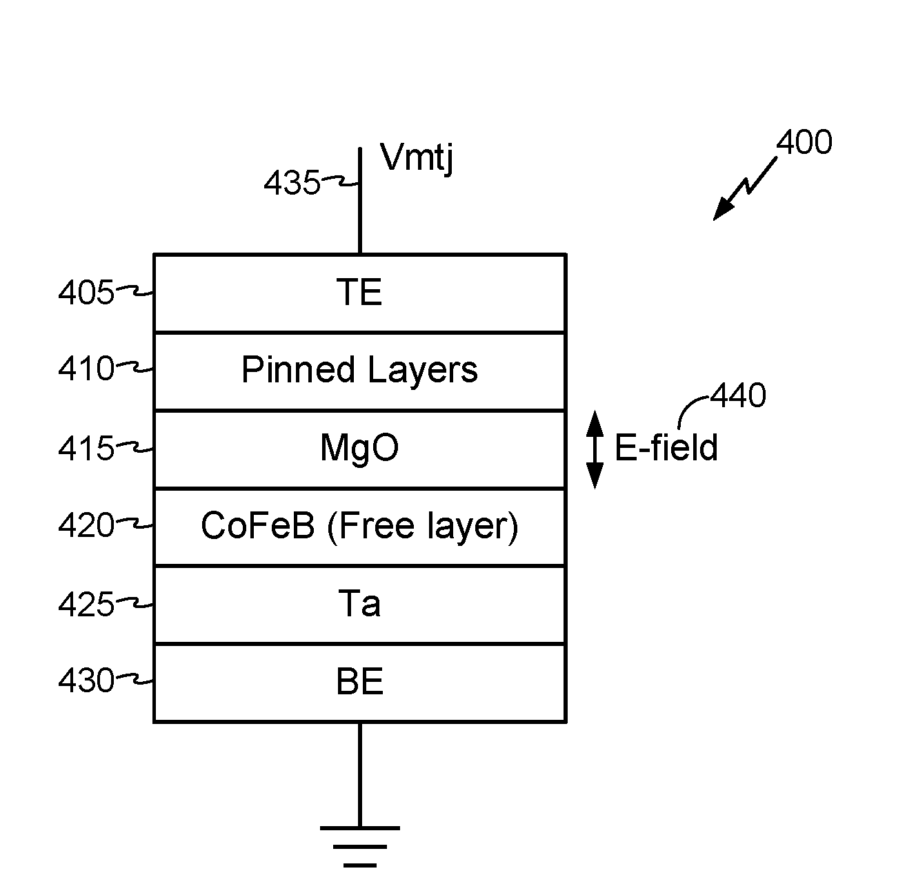
[0028]Methods and apparatus relating to spin-orbit-torque magnetoresistive random access memory with voltage-controlled anisotropy are provided. In an example, disclosed is a 3-terminal magnetic tunnel junction (MTJ) storage element that is programmed via a combination of voltage-controlled magnetic anisotropy (VCMA) and spin-orbit torque (SOT) techniques.

[0029]The exemplary apparatuses and methods disclosed herein advantageously address the long-felt industry needs, as well as other previously unidentified needs, and mitigate shortcomings of the conventional methods and apparatus. For example, an advantage provided by the disclosed apparatuses and methods herein is an improvement in efficiency over conventional devices. The disclosed devices also use less write energy, while having a design that is simpler and more scalable than conventional devices. The disclosed devices also have increased thermal stability without increasing required switching current, as critical sw...


PUM


Abstract

Methods and apparatus relating to spin-orbit-torque magnetoresistive random access memory with voltage-controlled anisotropy are disclosed. In an example, disclosed is a three-terminal magnetic tunnel junction (MTJ) storage element that is programmed via a combination of voltage-controlled magnetic anisotropy (VCMA) and spin-orbit torque (SOT) techniques. Also disclosed is a memory controller configured to program the three-terminal MTJ storage element via VCMA and SOT techniques. The disclosed devices improve efficiency over conventional devices by using less write energy, while having a design that is simpler and more scalable than conventional devices. The disclosed devices also have increased thermal stability without increasing required switching current, as critical switching current between states is essentially the same

Description

CROSS-REFERENCE TO RELATED APPLICATIONS[0001]The present application is a continuation of co-pending U.S. patent application Ser. No. 14 / 617,919, entitled “SPIN-ORBIT-TORQUE MAGNETORESISTIVE RANDOM ACCESS MEMORY WITH VOLTAGE-CONTROLLED ANISOTROPY,” filed Feb. 9, 2015, assigned to the assignee hereof, the contents of which are hereby expressly incorporated by reference in their entirety.INTRODUCTION[0002]This disclosure relates generally to electronics, and more specifically, but not exclusively, to methods and apparatus relating to spin-orbit-torque magnetoresistive random access memory with voltage-controlled anisotropy.[0003]Random access memory (RAM) is a ubiquitous component of modern digital circuit architectures. RAM can be a standalone device, or can be integrated in a device that uses the RAM, such as a microprocessor, microcontroller, application specific integrated circuit (ASIC), system-on-chip (SoC), and other like devices. RAM can be volatile or non-volatile. Volatile R...

Claims


Application Information

Patent Timeline
Patent Type & Authority Applications(United States)
IPC IPC(8): G11C11/16H01L43/10H01L43/12H01L43/02H01L43/08
CPCG11C11/1675H01L43/02H01L43/08H01L43/10G11C11/1673H01L43/12G11C11/161G11C11/18G11C8/005H10N50/01H10N50/10H10N50/80H10N50/85
Inventor LEE, KANGHOKAN, JIMMYKANG, SEUNG HYUK
Owner QUALCOMM INC
Why Eureka
Try Eureka