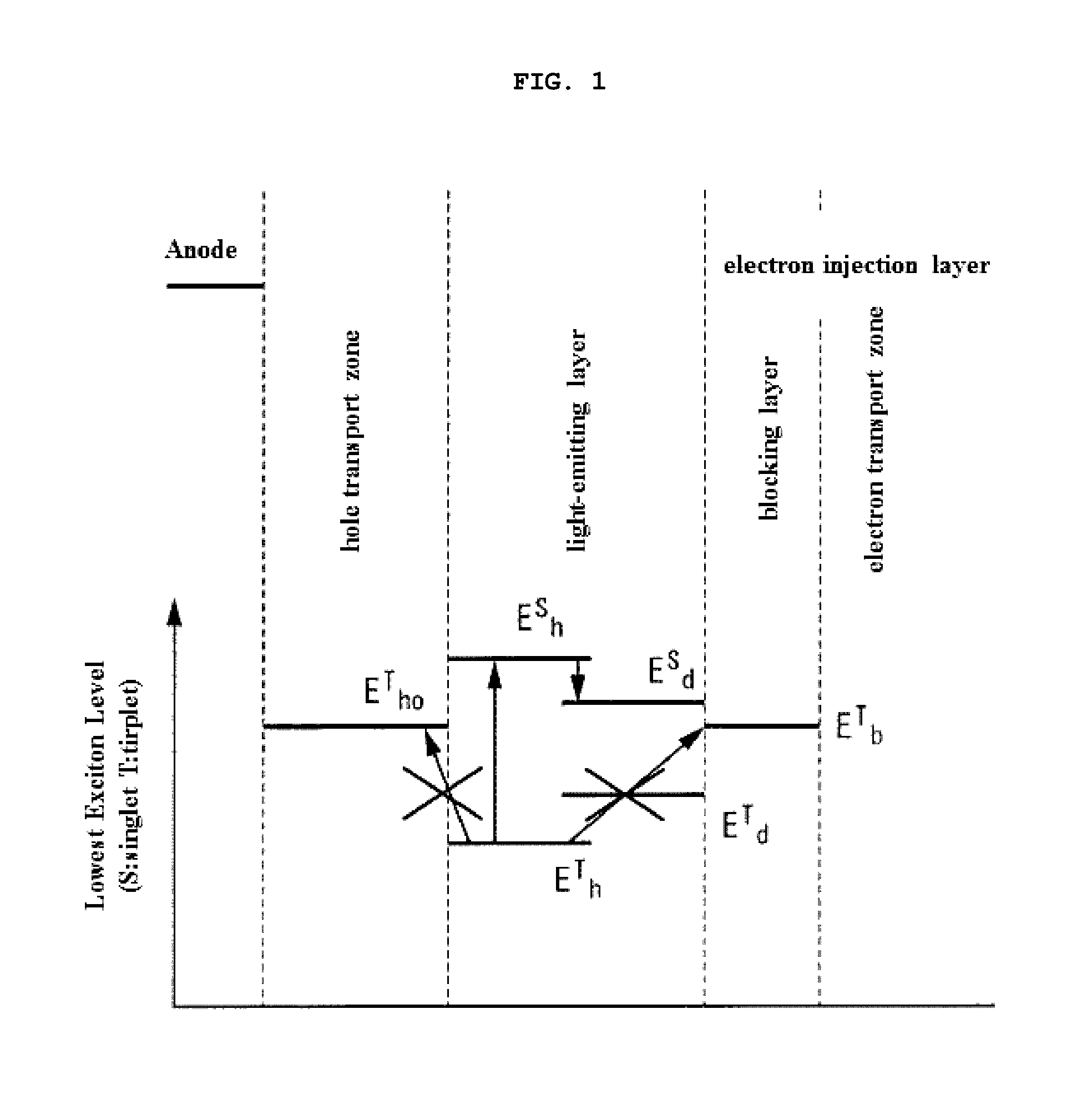
Organic light emitting diode
a light-emitting diode and organic technology, applied in the direction of luminescent compositions, semiconductor devices, chemistry apparatus and processes, etc., can solve the problems of reducing color purity and light emission efficiency, and placing a theoretical limit on the internal quantum efficiency of 25%, so as to achieve high luminous efficiency and increase the exciton density
- Summary
- Abstract
- Description
- Claims
- Application Information
AI Technical Summary
Benefits of technology
Problems solved by technology
Method used
Image

Examples
synthesis example 1
(7): Synthesis of [BD 1]
[0151]BD 1 was synthesized as illustrated in the following Reaction Scheme 7:
[0152]In a 250-ml round-bottom flask reactor, a mixture of (5.0 g, 0.009 mol), (4-tert-butylphenyl)-phenylamine (4.7 g, 0.021 mol), palladium (II) acetate (0.08 g, 0.4 mmol), sodium tert-butoxide (3.4 g, 0.035 mol), tri-tert-butyl phosphine (0.07 g, 0.4 mmol), and toluene (60 ml) was stirred for 2 hrs under reflux. After completion of the reaction, the reaction mixture was cooled to room temperature and then extracted with dichloromethane and water. The organic layer thus formed was separated, dried over magnesium sulfate, and concentrated in a vacuum. The concentrate was purified by column chromatography and recrystallized in dichloromethane and acetone to yield as a solid (2.9 g, 38%).
[0153]MS (MALDI-TOF): m / z 852.41 [M+]
example 1-3
Fabrication of Organic Light-Emitting Diode
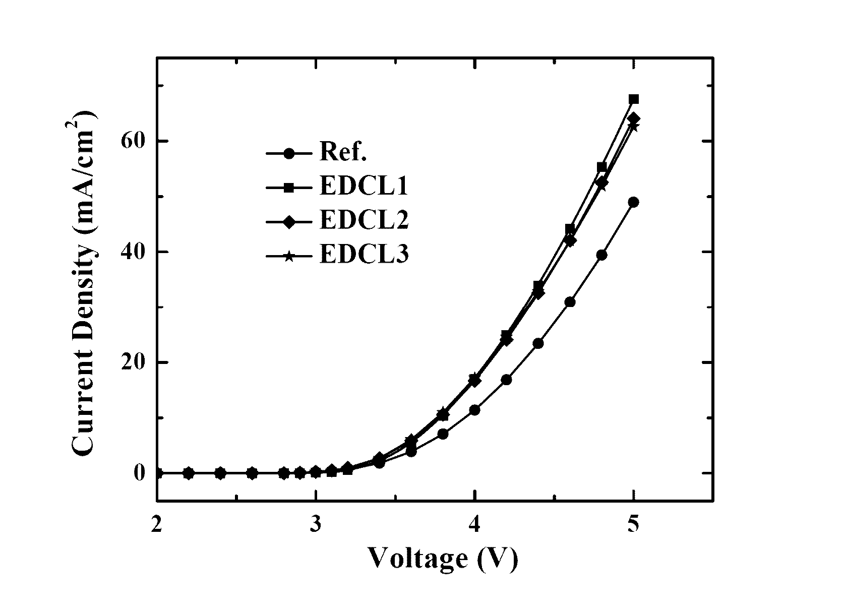
[0154]An ITO glass substrate was patterned to have a luminescent area of 2 mm×2 mm and cleansed. The ITO glass was mounted in a vacuum chamber that was then set to have a base pressure of 1×10⁻⁷ torr. On the ITO glass substrate, films of DNTPD (400 Å) and α-NPD (200 Å) were formed in that order. A light-emitting layer (200 Å) was formed of a mixture of BH and BD 1 (weight ratio 97:3). Then, the compounds shown in Table 1 were deposited to form an electron-density-controlling layer (50 Å thick), on which [Chemical Formula E-2] for an electron transport layer (250 Å), [Chemical Formula E-1] for an electron injection layer (5 Å), and Al (1000 Å) were deposited in the order to fabricate an organic light-emitting diode. The organic light-emitting diode thus obtained was measured at 10 mA / cm2 for luminescence properties.
[0155]In addition, triplet energy values of each the host materials and the electron-density-controlling layer materials are giv...
example 4
Fabrication of Organic Light-Emitting Diode
[0161]An organic light-emitting diode was fabricated in the same manner as in Examples 1 to 3, with the exception that [BD2] was used, instead of [BD1], as a dopant in the light-emitting layer. The organic light-emitting diode was measured at 10 mA / cm2 for luminescence properties. The structure of [BD2] is as follows:
PUM
| Property | Measurement | Unit |
|---|---|---|
| triplet energy | aaaaa | aaaaa |
| triplet energy | aaaaa | aaaaa |
| wavelength range | aaaaa | aaaaa |
Abstract
Description
Claims
Application Information
 - R&D
- Intellectual Property
- Life Sciences
- Materials
- Tech Scout
- Unparalleled Data Quality
- Higher Quality Content
- 60% Fewer Hallucinations
Browse by: Latest US Patents, China's latest patents, Technical Efficacy Thesaurus, Application Domain, Technology Topic, Popular Technical Reports.
© 2025 PatSnap. All rights reserved.Legal|Privacy policy|Modern Slavery Act Transparency Statement|Sitemap|About US| Contact US: help@patsnap.com