Diamond crystal, diamond devices, magnetic sensor, magnetic sensor system, and method for manufacturing sensor array

a technology of diamond devices and diamond crystals, applied in the direction of crystal growth process, polycrystalline material growth, instruments, etc., can solve the problem of difficult to cause fluorescence process, and achieve the effect of enhanced contrast and high sensitivity

Active Publication Date: 2016-11-17
JAPAN SCI & TECH CORP +1
View PDF3 Cites 20 Cited by
  • Summary
  • Abstract
  • Description
  • Claims
  • Application Information

AI Technical Summary

Benefits of technology

[0039]The diamond crystal according to the present invention enables almost 100% of the complex (NV center) of the nitrogen (N) substituted with the carbon atom and the vacancy (V) located adjacent to the nitrogen to be in a negatively charged state (NV−). In addition, spin states of the NV− centers can be aligned in one direction, and as a result, a peak of an optically detected magnetic resonance (ODMR: Optically Detected Magnetic Resonance) signal becomes sharp, and besides, a contrast is also enhanced.
[0040]Furthermore, the diamond device according to the present invention can keep the NV center formed in the above described diamond crystal in a negatively charged state (NV−).
[0041]As a result, the magnetic sensor that is provided with the diamond device according to the present invention enables two-dimensional magnetic measurement at ordinary temperature in the atmosphere to be carried out with high sensitivity as compared with a conventional one.

Problems solved by technology

However, when it has the electron spin of |1> or |−1> in the ground state, some of the electrons after excitation pass through a singlet state and returns to the ground state, which makes it difficult to cause a fluorescence process.

Method used


Image

  • Diamond crystal, diamond devices, magnetic sensor, magnetic sensor system, and method for manufacturing sensor array
  • Diamond crystal, diamond devices, magnetic sensor, magnetic sensor system, and method for manufacturing sensor array
  • Diamond crystal, diamond devices, magnetic sensor, magnetic sensor system, and method for manufacturing sensor array

Examples


example 1

[0132]FIG. 11 is a view for conceptually describing an example of a process for manufacturing a sensor array according to the present invention.

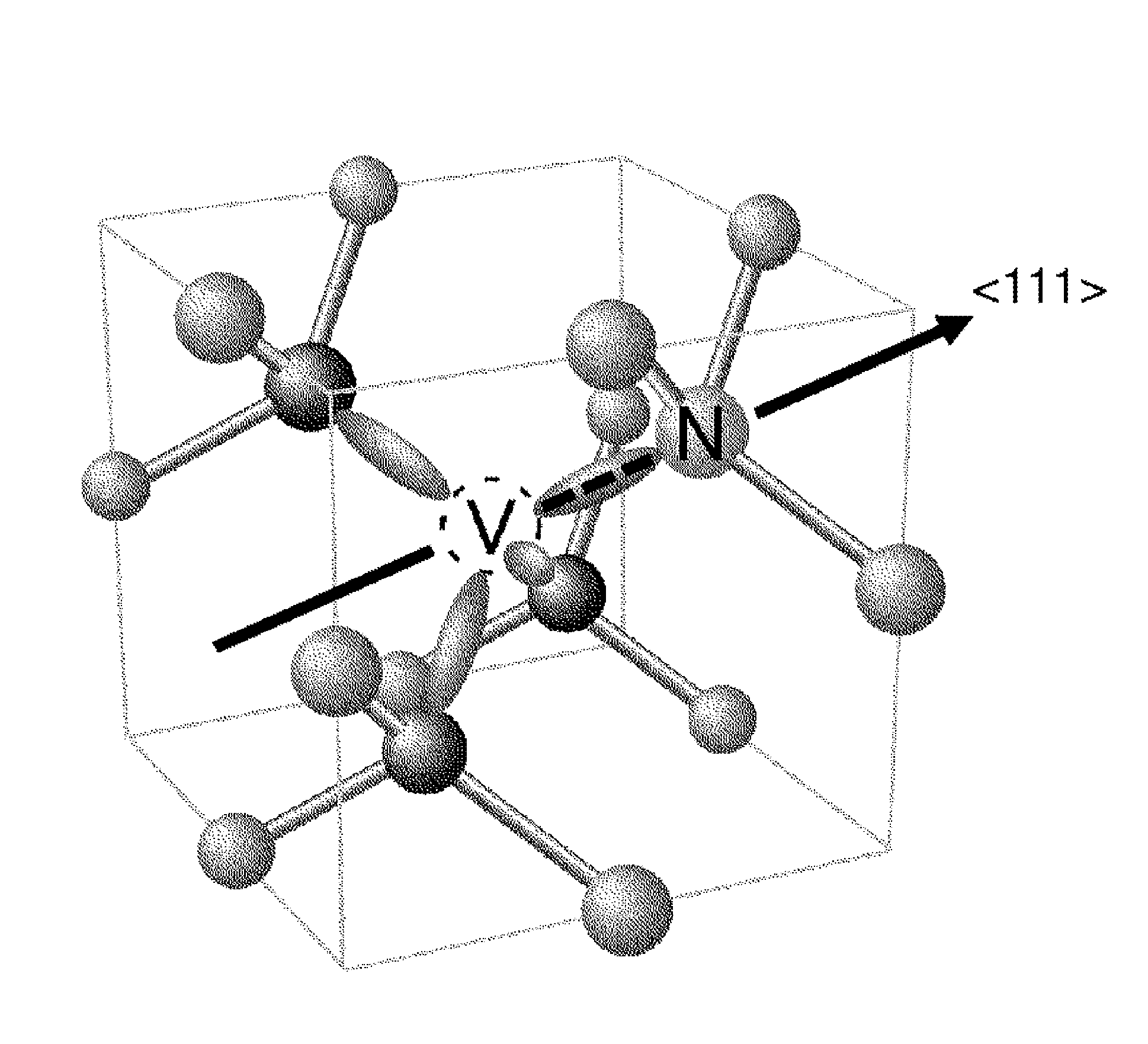
[0133]Firstly, a diamond substrate 10 of which the principal surface is the (111) face is prepared (FIG. 11(A)), and a first mask 12 is formed on the principal surface of this diamond substrate 10 so that the above described first regions are two-dimensionally and periodically arrayed in a plane (FIG. 11(B)). Then, the peripheries of the regions that have been covered with this first mask 12 are removed by etching, and columnar portions 11 are formed that are two-dimensionally and periodically arrayed (FIG. 11(C)). Incidentally, this substrate 10 is a p-type single crystal diamond substrate that is doped, for instance, with boron (B); and in the case of the p-type, is preferably a p− type (for instance, substrate having dope amount of 10×1016 cm−3 or less in terms of boron concentration), or is more preferably a substrate (i-type) having res...

example 2

[0137]FIG. 12 is a view for conceptually describing an example of another process for manufacturing a sensor array according to the present invention.

[0138]A single crystal diamond substrate 10a is prepared of which the principal surface is the (111) face (FIG. 12(A)), and on the principal surface of this diamond substrate 10a, a single crystal diamond thin film 10b of which the conductivity type is, for instance, a p-type (or i-type) is formed by the CVD method (FIG. 12(B)). Incidentally, in the case of the p-type, the single crystal diamond thin film 10b is preferably a p− type (for instance, thin film having dope amount of 10×1016 cm−3 or less in terms of boron concentration), or preferably has the resistivity that is close to that of an intrinsic semiconductor. This diamond substrate 10a and the diamond thin film 10b correspond to the above described diamond substrate 10.

[0139]Subsequent steps are similar to the steps described with reference to FIG. 11, and includes: forming a ...

example 3

[0144]FIG. 13 is a view for conceptually describing an example of another process for manufacturing a sensor array according to the present invention. In this process example, the NV center is not formed by the ion implantation method, but is formed by being doped with nitrogen, while the single crystal diamond thin film 10b is formed by the CVD method.

[0145]A single crystal diamond substrate 10a is prepared of which the principal surface is the (111) face (FIG. 13(A)), and a single crystal diamond thin film 10b that is doped with the nitrogen (N) and has the principal surface of the (111) face is formed on the principal surface of this diamond substrate 10a, with the CVD method (FIG. 13(B)). This diamond substrate 10a and the diamond thin film 10b correspond to the above described diamond substrate 10. A mixed gas of hydrogen, methane and nitrogen is used as a process gas, for film formation of the single crystal diamond thin film 10b. Nitrogen is taken in during a CVD reaction, an...


PUM

PropertyMeasurementUnit
off-angleaaaaaaaaaa
frequencyaaaaaaaaaa
frequenciesaaaaaaaaaa

Abstract

A diamond crystal according to the present invention has an NV region containing a complex (NV center) of nitrogen substituted with a carbon atom and a vacancy located adjacent to the nitrogen, on a surface or in the vicinity of the surface, wherein the NV region has a donor concentration equal to or higher than the concentration of the NV centers, or a crystal of the NV region is a {111} face or a face having an off-angle that is ±10 degrees or less against the {111} face, and a principal axis of the NV center is a <111> axis that is perpendicular to the {111} face. Such a diamond crystal enables almost 100% of the NV center to be a state (NV−) of having a negative electric charge, and spin states of the NV− centers to be aligned in one direction.

Description

TECHNICAL FIELD[0001]The present invention relates to a technology for enabling high-sensitivity magnetic sensor, and in particular, relates to a diamond crystal and film that enables the high-sensitivity magnetic measurement at room temperature in the atmosphere, a magnetic sensor using the same, and the like.BACKGROUND ART[0002]Diamond can be said to be a specific crystal lattice in which a color center in a crystal behaves like so called “atoms (trapped atoms) in low temperature and a vacuum” in room temperature and the atmosphere. A nitrogen-vacancy complex (NV center) that is formed in the specific crystal lattice, or diamond, is one type of color center, and involves nitrogen (N) substituted with carbon and an atomic vacancy (V) that is positioned adjacent to this nitrogen, as is illustrated in FIG. 1, and has a spin S=1.[0003]An NV− center, which is the NV center in a negatively charged state once it captures an electron, is only one solid characterized by the fact that a sin...

Claims


Application Information

Patent Timeline
Patent Type & Authority Applications(United States)
IPC IPC(8): G01R33/032C30B25/20C30B25/02G01R33/00C30B29/04
CPCG01R33/032G01R33/0052C30B25/20C30B25/02C30B29/04G01R33/0094G01R33/1284G01N24/10G01R33/24G01R33/323
Inventor HATANO, MUTSUKOIWASAKI, TAKAYUKIMIZUOCHI, NORIKAZUMAKINO, TOSHIHARUKATO, HIROMITSUYAMASAKI, SATOSHI
Owner JAPAN SCI & TECH CORP
Why Eureka
Try Eureka