Optimized 2x2 3db multi-mode interference coupler

a multi-mode interference and coupler technology, applied in the field of optical couplers, to achieve the effect of reducing optical loss

Active Publication Date: 2016-12-29
NOKIA SOLUTIONS & NETWORKS OY
View PDF3 Cites 9 Cited by
  • Summary
  • Abstract
  • Description
  • Claims
  • Application Information

AI Technical Summary

Benefits of technology

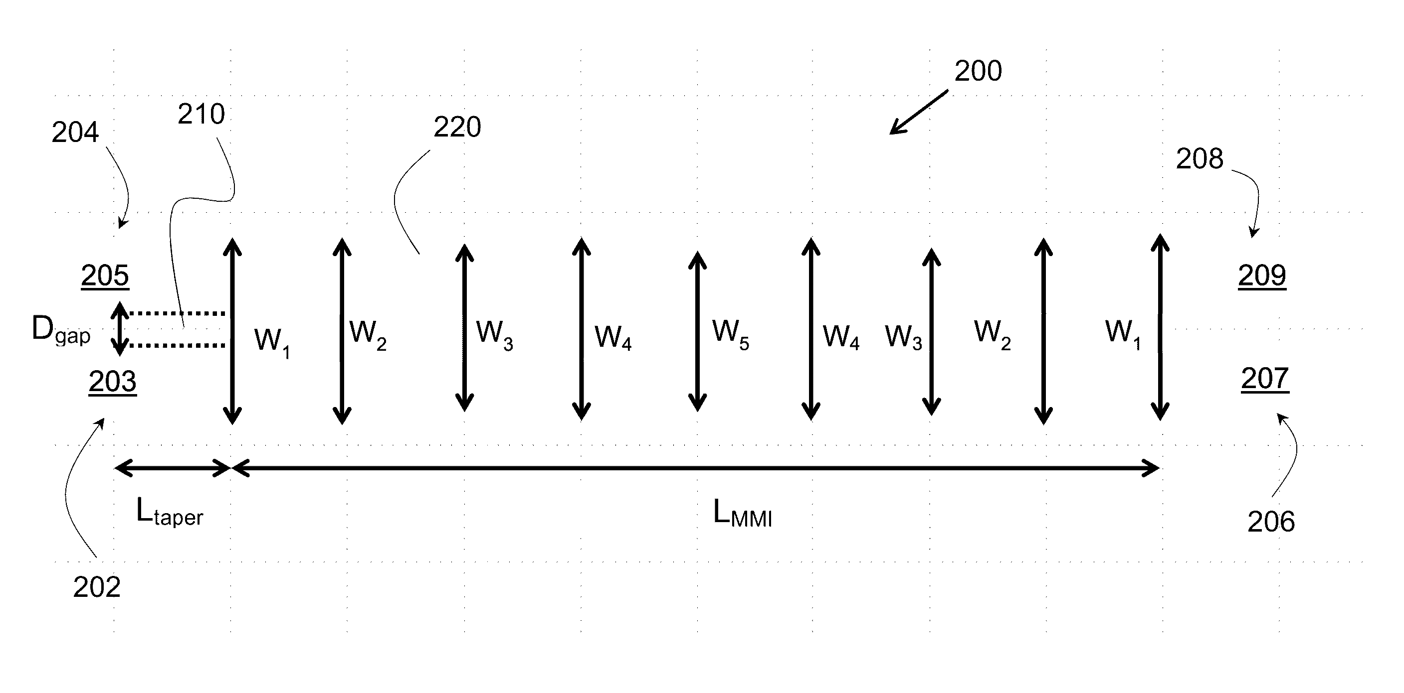
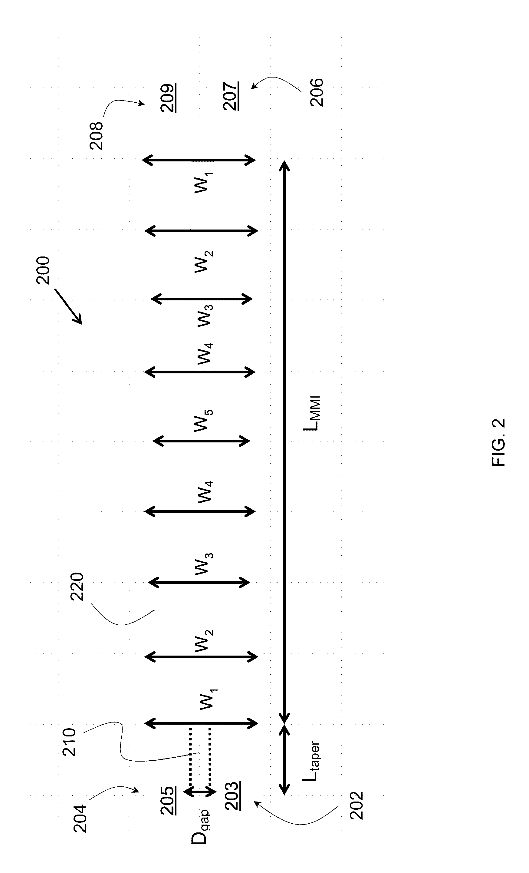
[0006]In another embodiment, the length Ltaper is tuned to reduce optical loss.

Problems solved by technology

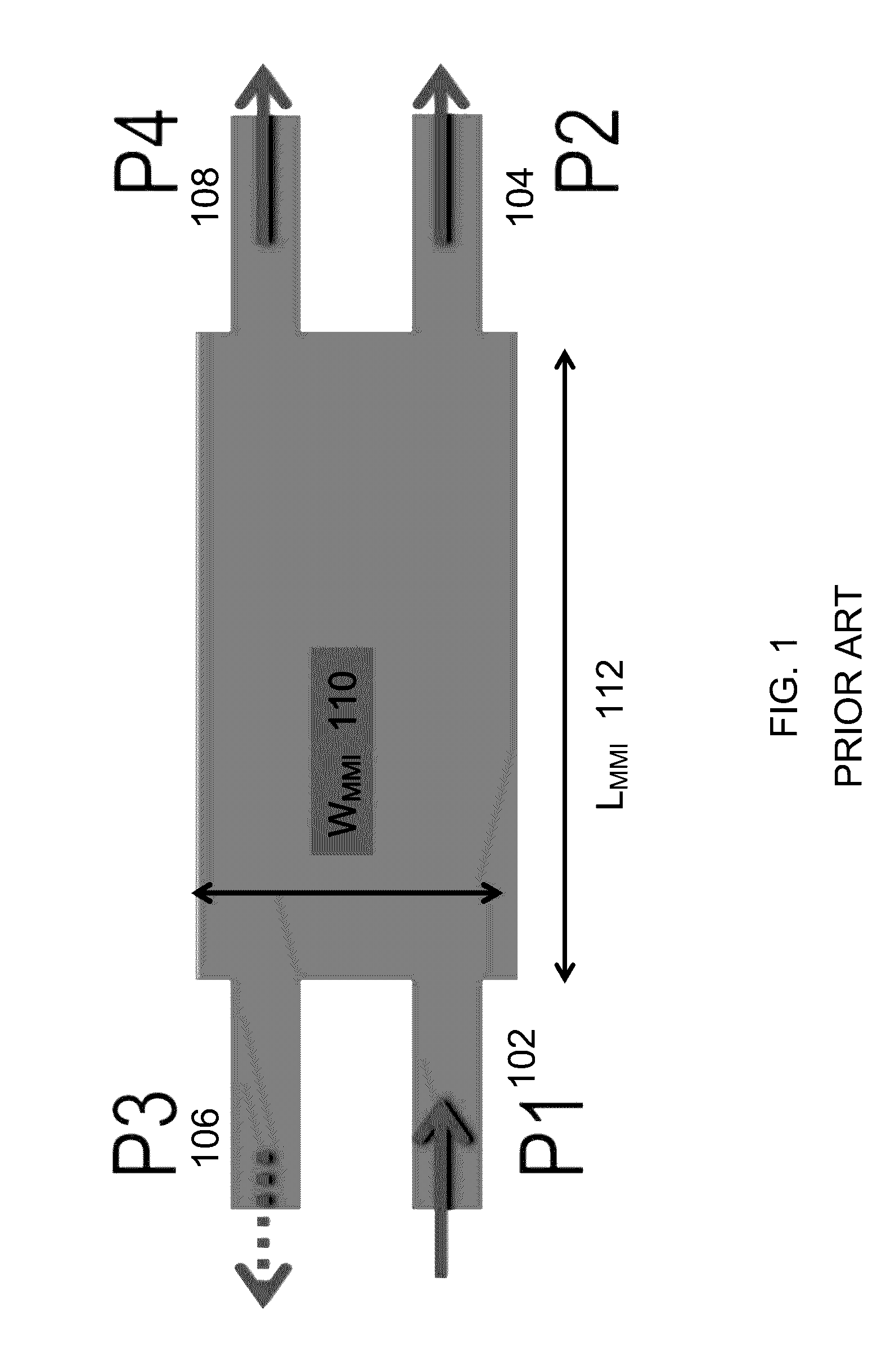
The main challenge to replace a 3 dB directional coupler is matching or improving on the insertion loss and phase error.

Method used


Image

  • Optimized 2x2 3db multi-mode interference coupler
  • Optimized 2x2 3db multi-mode interference coupler
  • Optimized 2x2 3db multi-mode interference coupler

Examples


Embodiment Construction

Acronyms

[0026]A list of acronyms and their usual meanings in the present document (unless otherwise explicitly stated to denote a different thing) are presented below.

[0027]AMR Adabatic Micro-Ring

[0028]APD Avalanche Photodetector

[0029]ARM Anti-Reflection Microstructure

[0030]ASE Amplifled Spontaneous Emission

[0031]BER Bit Error Rate

[0032]BOX Buried Oxide

[0033]CMOS Complementary Metal-Oxide-Semiconductor

[0034]CMP Chemical-Mechanical Planarization

[0035]DBR Distributed Bragg Reflector

[0036]DC (optics) Directional Coupler

[0037]DC (electronics) Direct Current

[0038]DCA Digital Communication Analyzer

[0039]DRC Design Rule Checking

[0040]DSP Digital Signal Processor

[0041]DUT Device Under Test

[0042]ECL External Cavity Laser

[0043]E / O Electro-optical

[0044]FDTD Finite Difference Time Domain

[0045]FFE Feed-Forward Equalization

[0046]FOM Figure of Merit

[0047]FSR Free Spectral Range

[0048]FWHM Full Width at Half Maximum

[0049]GaAs Gallium Arsenide

[0050]InP Indium Phosphide

[0051]LiNO3 Lithium Niobate

[0052...


PUM


Abstract

An optimized SOI 2×2 multimode interference (MMI) coupler is designed by use of the particle swarm optimization (PSO) algorithm. Finite Difference Time Domain (FDTD) simulation shows that, within a footprint of 9.4×1.6 μm2, <0.1 dB power unbalance and <1 degree phase error are achieved across the entire C-band. The excess loss of the device is <0.2 dB.

Description

FIELD OF THE INVENTION[0001]The invention relates to optical couplers in general and particularly to a multimode interference coupler.BACKGROUND OF THE INVENTION[0002]A 2×2 3 dB multimode interference (MMI) coupler is a fundamental building block in photonic integrated circuits (PIC). It behaves as a 3 dB power splitter such as a y-junction. It also provides 90-degree phase difference between the two output ports, which is an attractive feature in many applications such as switches and coherent communications. The broadband wavelength response also makes it a better candidate for directional couplers (DC) when it comes to 3 dB power coupling. The main challenge to replace a 3 dB directional coupler is matching or improving on the insertion loss and phase error. A small footprint is also very desirable for large-scale photonic integration.[0003]There is a need for improved multimode interference couplers.SUMMARY OF THE INVENTION[0004]According to one aspect, the invention features a ...

Claims


Application Information

Patent Timeline
Patent Type & Authority Applications(United States)
IPC IPC(8): G02B6/293G02B27/00
CPCG02B27/0012G02B6/29344G02B6/2813G02B6/1228G02B6/125G02B2006/12147G02B2006/1215G02B2006/12159
Inventor MA, YANGJIN
Owner NOKIA SOLUTIONS & NETWORKS OY
Why Eureka
Try Eureka