Shadow-effect compensated fabrication of magnetic tunnel junction (MTJ) elements

a technology of shadow effect and fabrication, applied in the direction of magnetic field-controlled resistors, electrical devices, semiconductor devices, etc., can solve the problems of poor mtj performance, rie processes are known to create damage zones around the perimeter of mtj, and the stt-mtj has a large operational power consumption, so as to reduce the size of the free layer, and enhance the mtj operational margin

Inactive Publication Date: 2017-02-16
QUALCOMM INC
View PDF1 Cites 20 Cited by
  • Summary
  • Abstract
  • Description
  • Claims
  • Application Information

AI Technical Summary

Benefits of technology

[0011]Aspects of the disclosure involve shadow-effect compensated fabrication of magnetic tunnel junction (MTJ) elements. Providing shadow-effect compensated fabrication of MTJ elements can provide reduced free layer sizing for enhanced MTJ operational margin. Related devices, methods, memory systems are also disclosed. Reducing the size of the free layer during fabrication of an MTJ allows less write current to write data to the MTJ, thus increasing write current operational margin of the MTJ. In certain aspects disclosed herein, to reduce the size of the free layer during fabrication of an MTJ to provide enhanced write and retention symmetry, ion beam etching (IBE) fabrication processes are employed. IBE has advantages of employing a simple hard mask without chemical etching. During the IBE fabrication process, an ion beam is controlled to be directed at an angle of incidence towards an MTJ disposed in a semiconductor wafer to fabricate the free layer to be smaller in size than a pinned layer. To avoid an asymmetrical footing being fabricated in the free layer formed in the MTJ due to a shadow-effect of neighboring MTJs blocking an ion beam at certain angles, the ion beam directed at the MTJ is shadow-effect compensated. The angle of incidence of the ion beam directed at the MTJ is varied as the semiconductor wafer supporting the MTJ is rotated during fabrication. In this manner, as an example, the angle of incidence of the ion beam can be controlled to be less steep when another MTJ is in the directional line of the ion beam and the MTJ being fabricated. Thus, the free layer is etched more uniformly in the MTJ while avoiding increased etching damage that would result from providing only a higher angle of incidence of the ion beam during etching without variation during rotation of the MTJ.

Problems solved by technology

Write asymmetry causes greater operational power consumption by the STT-MTJ 100.
RIE processes are known to create damage zones around the perimeter of the MTJ.
Etching damage in the transition metals (i.e., the pinned layer 108, the free layer 112, and the bottom and top electrodes 106, 110) in the MTJ can affect factors such as a tunnel magnetoresistance (TMR) ratio and energy bather (Eb) variations, which can result in poor MTJ performance.
Also, as MTJs become scaled down, such as in high-density MRAMs, these damages zones limit the amount of downscaling.

Method used


Image

  • Shadow-effect compensated fabrication of magnetic tunnel junction (MTJ) elements
  • Shadow-effect compensated fabrication of magnetic tunnel junction (MTJ) elements
  • Shadow-effect compensated fabrication of magnetic tunnel junction (MTJ) elements

Examples


Embodiment Construction

[0027]With reference now to the drawing figures, several exemplary aspects of the present disclosure are described. The word “exemplary” is used herein to mean “serving as an example, instance, or illustration.” Any aspect described herein as “exemplary” is not necessarily to be construed as preferred or advantageous over other aspects.

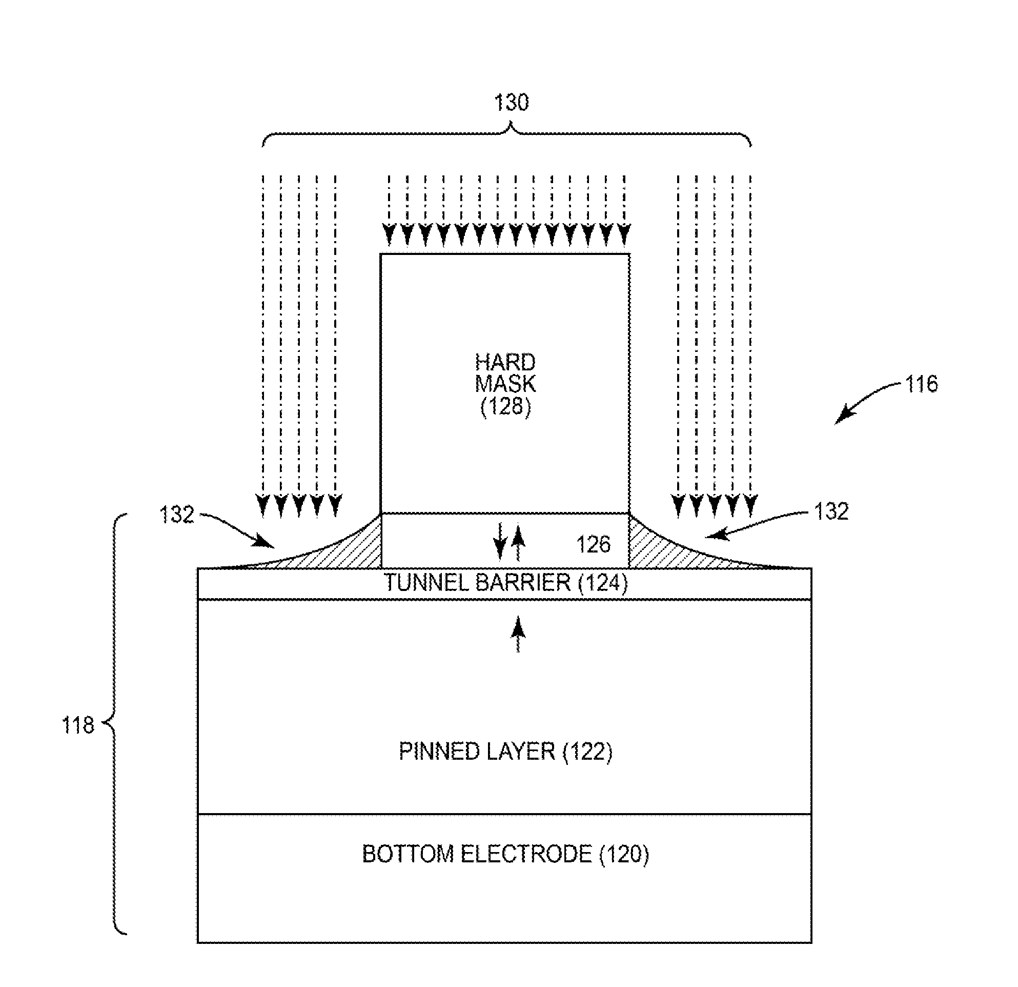
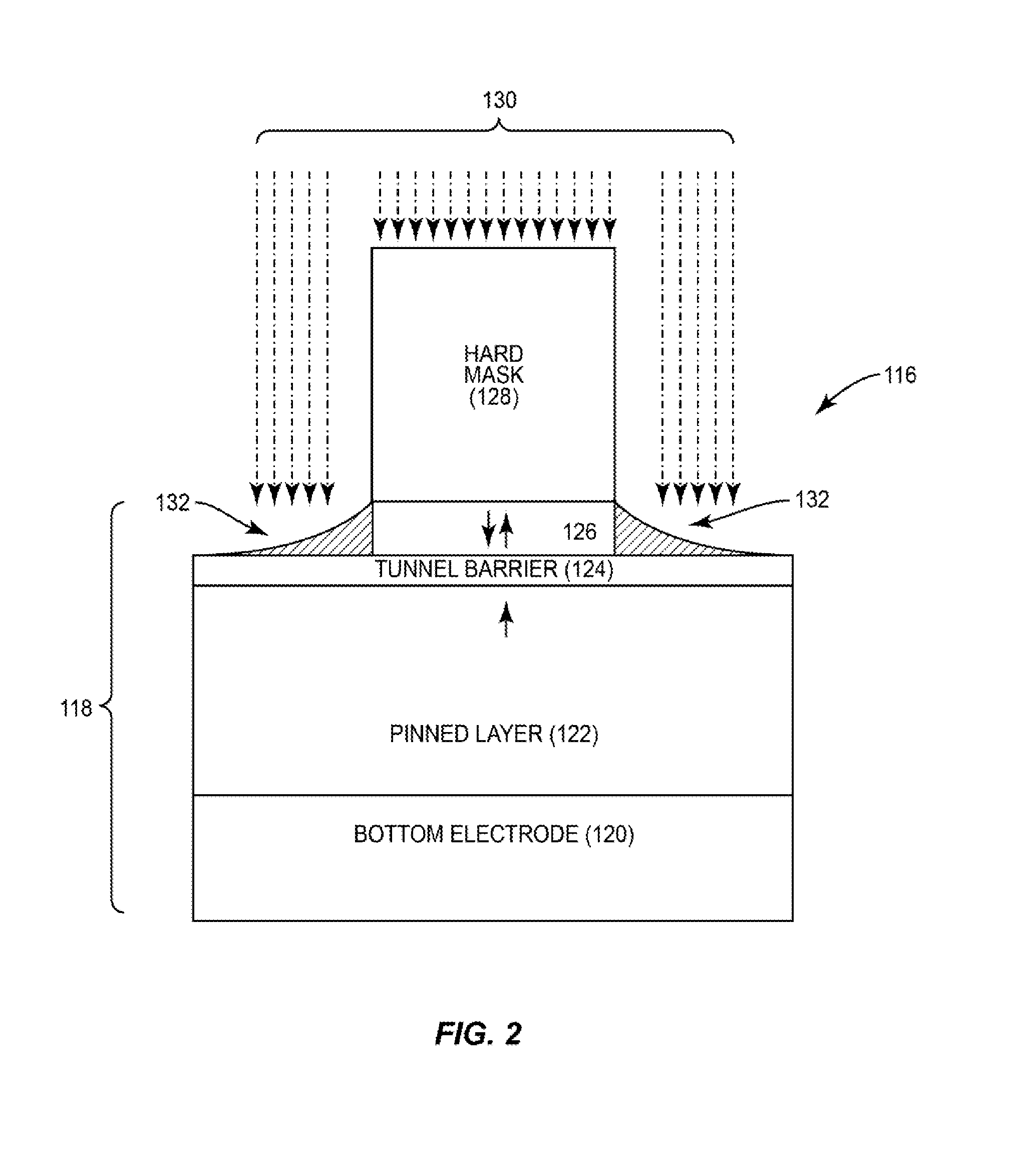
[0028]Aspects of the disclosure involve shadow-effect compensated fabrication of magnetic tunnel junction (MTJ) elements. Providing shadow-effect compensated fabrication of MTJ elements can provide reduced free layer sizing for enhanced MTJ operational margin. Related devices, methods, memory systems are also disclosed. Reducing the size of the free layer during fabrication of an MTJ allows less write current to write data to the MTJ, thus increasing write current operational margin of the MTJ. In certain aspects disclosed herein, to reduce the size of the free layer during fabrication of an MTJ to provide enhanced write and retention symmetry, ion be...


PUM


Abstract

Shadow-effect compensated fabrication of magnetic tunnel junction (MTJ) semiconductor elements is disclosed. Providing shadow-effect compensated fabrication of MTJ elements can provide reduced free layer sizing for enhanced MTJ operational margin. In certain aspects, to reduce size of a free layer during fabrication of an MTJ to provide enhanced write and retention symmetry, ion beam etching (IBE) fabrication process is employed to fabricate a free layer smaller than the pinned layer. To avoid asymmetrical footing being fabricated in free layer due to shadow-effect of neighboring MTJs, an ion beam directed at the MTJ is shadow-effect compensated. The angle of incidence of the ion beam directed at the MTJ is varied as the MTJ is rotated to be less steep when another MTJ is in directional line of the ion beam and the MTJ being fabricated. Thus, the free layer is etched more uniformly in the MTJ while avoiding increased etching damage.

Description

BACKGROUND[0001]I. Field of the Disclosure[0002]The technology of the disclosure relates generally to fabrication of magnetic tunnel junction (MTJ) elements in semiconductor devices, and more particularly to MTJ etching.[0003]II. Background[0004]Semiconductor storage devices are used in integrated circuits (ICs) in electronic devices to provide data storage. One example of a semiconductor storage device is a magnetic random access memory (MRAM). MRAM is non-volatile memory in which data is stored by programming a magnetic tunnel junction (MTJ) as part of an MRAM bit cell. One advantage of an MRAM is that MTJs in MRAM bit cells can retain stored information even when power is turned off. This is because data is stored in the MTJ as a small magnetic element rather than an electric charge or current.[0005]In this regard, an MTJ comprises a free ferromagnetic layer (“free layer”) disposed above a fixed or pinned ferromagnetic layer (“pinned layer”). The free and pinned layers are separa...

Claims


Application Information

Patent Timeline
Patent Type & Authority Applications(United States)
IPC IPC(8): H01L43/12H01L43/08H01L27/22H01L43/02
CPCH01L43/12H01L27/222H01L43/08H01L43/02H10B61/22H10N50/10H10N50/01H10B61/00H10N50/80
Inventor CHEN, WEI-CHUANLU, YUPARK, CHANDOKANG, SEUNG HYUK
Owner QUALCOMM INC
Why Eureka
Try Eureka