An electron transport material and an organic electroluminescence device comprising the same

an electron transport material and electron transport technology, applied in the direction of solid-state devices, organic chemistry, chemistry apparatus and processes, etc., can solve the problems of reducing color purity, moving to other layers, and failing to disclose an electron transport device using the compound as a transport material, etc., to achieve high efficiency and long life

Inactive Publication Date: 2017-03-16
ROHM & HAAS ELECTRONICS MATERIALS LLC
View PDF1 Cites 11 Cited by
  • Summary
  • Abstract
  • Description
  • Claims
  • Application Information

AI Technical Summary

Benefits of technology

[0020]By using the electron transport material according to the present invention, an organic EL device with high efficiency and long lifespan is provided, and it is possible to produce a display device or a lighting device using the organic EL device.
[0021]FIG. 1 illustrates a schematic sectional view of an organic electroluminescent device comprising the electron transport layer comprising the electron transport material according to one embodiment of the present invention.
[0022]FIG. 2 illustrates a comparison of current efficiency between an organic electroluminescent device according to one embodiment of the present invention and a conventional organic electroluminescent device.
[0023]FIG. 3 illustrates an energy gap relationship among the layers of the organic electroluminescent device according to one embodiment of the present invention.
[0024]Hereinafter, the present invention will be described in detail. However, the following description is intended to explain the invention, and is not meant in any way to restrict the scope of the invention.
[0025]Hereinafter, the compound represented by formula 1 will be described in detail.

Problems solved by technology

However, Alq3 has problems in that it moves to other layers and shows reduction of color purity when used in blue light-emitting devices.
However, it fails to disclose an organic EL device using the compound as an electron transport material.

Method used


Image

  • An electron transport material and an organic electroluminescence device comprising the same
  • An electron transport material and an organic electroluminescence device comprising the same
  • An electron transport material and an organic electroluminescence device comprising the same

Examples


example 1

DEVICE EXAMPLE 1

Production of an OLED Device Comprising the Electron Transport Material According to the Present Invention

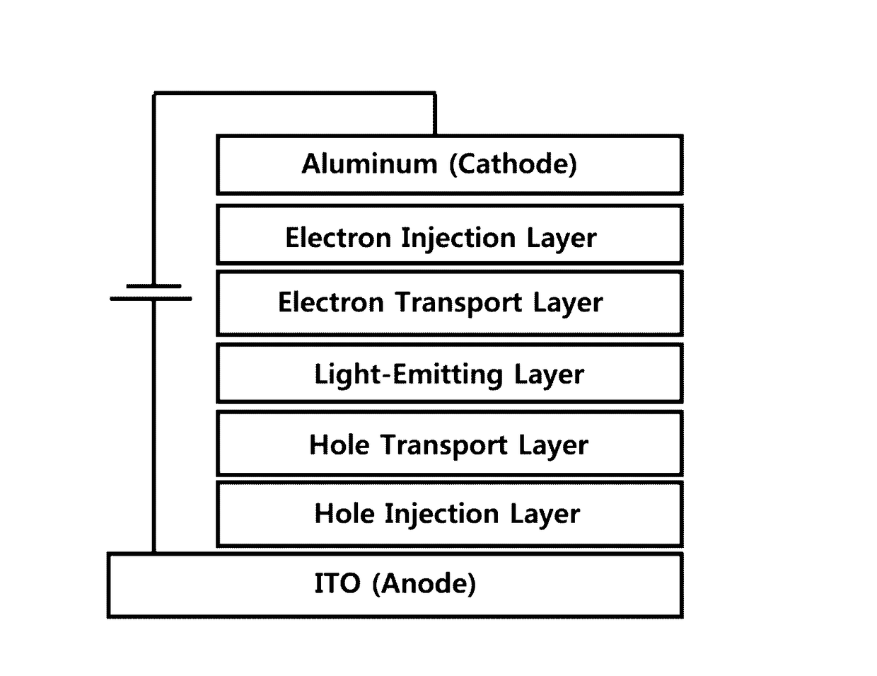
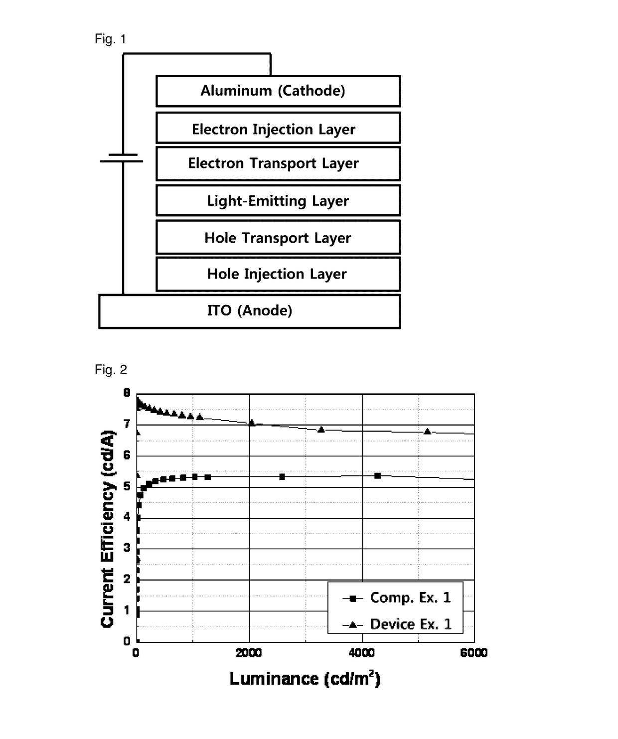
[0063]An OLED device was produced using the electron transport material of the present invention. A transparent electrode indium tin oxide (ITO) thin film (15 Ω / sq) on a glass substrate for an OLED device (Geomatec Co. LTD., Japan) was subjected to an ultrasonic washing with trichloroethylene, acetone, ethanol, and distilled water, sequentially, and was then stored in isopropanol. The ITO substrate was then mounted on a substrate holder of a vacuum vapor depositing apparatus. N4,N4′-diphenyl-N4,N4′-bis(9-phenyl-9H-carbazol-3-yl)-[1,1′-biphenyl]-4,4′-diamine was introduced into a cell of the vacuum vapor depositing apparatus, and the pressure in the chamber of the apparatus was then controlled to 10−6 torr. Thereafter, an electric current was applied to the cell to evaporate the introduced material, thereby forming hole injection layer 1 having a thickness of 60 n...

example 2

DEVICE EXAMPLE 2

Production of an OLED Device Comprising the Electron Transport Material According to the Present Invention

[0064]An OLED device was produced in the same manner as in Device Example 1, except that compound ETL-78 was used in the electron transport layer.

example 3

Device Example 3

Production of an OLED Device Comprising the Electron Transport Material According to the Present Invention

[0065]An OLED device was produced in the same manner as in Device Example 1, except that compound ETL-80 was used in the electron transport layer.


PUM

PropertyMeasurementUnit
pressureaaaaaaaaaa
thicknessaaaaaaaaaa
thicknessaaaaaaaaaa

Abstract

The present invention relates to an organic electroluminescent device comprising an electron transport material which comprises a compound having a specific structure. The organic electroluminescent device comprising the electron transport material of the present invention provides low driving voltage, high luminous efficiency, excellent lifespan characteristics, and excellent color coordination to efficiently emit blue light.

Description

TECHNICAL FIELD[0001]The present invention relates to an electron transport material having improved electron transport ability, and an organic electroluminescent device comprising the same.BACKGROUND ART[0002]An electroluminescent (EL) device is a self-light-emitting device with the advantages of providing a wider viewing angle, a greater contrast ratio, and a faster response time. The first organic EL device was developed by Eastman Kodak, by using small aromatic diamine molecules and aluminum complexes as materials for forming a light-emitting layer (see Appl. Phys. Lett. 51, 913, 1987).[0003]An organic EL device changes electric energy into light by the injection of a charge into an organic light-emitting material, and commonly comprises an anode, a cathode, and an organic layer formed between the two electrodes. The organic layer of the organic EL device may be composed of a hole injection layer (HIL), a hole transport layer (HTL), an electron blocking layer (EBL), a light-emit...

Claims


Application Information

Patent Timeline
Patent Type & Authority Applications(United States)
IPC IPC(8): H01L51/00C07D409/14C07D403/14C07D405/14C07D403/04C07D403/10
CPCH01L51/0067C07D403/04H01L51/0072C07D403/10H01L51/0052H01L51/5076C07D405/14H01L51/0073C07D409/14H01L51/0074H01L51/5072C07D403/14C07D401/14C07F7/0812C07D407/14H10K85/654H10K85/6572H10K50/165H10K50/16C07D405/04C07F7/10C07D409/10H10K85/615H10K85/6574H10K85/6576
Inventor KIM, CHI-SIKJUN, JI-SONGCHO, YOUNG-JUNCHOI, KYUNG-HOONCHO, SANG-HEESHIM, JAE-HOONNA, HONG-YEOP
Owner ROHM & HAAS ELECTRONICS MATERIALS LLC
Why Eureka
Try Eureka