Method for manufacturing silicon carbide semiconductor device and silicon carbide semiconductor device
- Summary
- Abstract
- Description
- Claims
- Application Information
AI Technical Summary
Benefits of technology
Problems solved by technology
Method used
Image

Examples
example
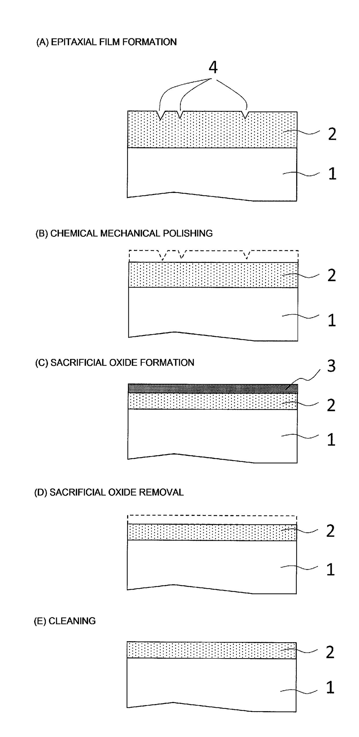
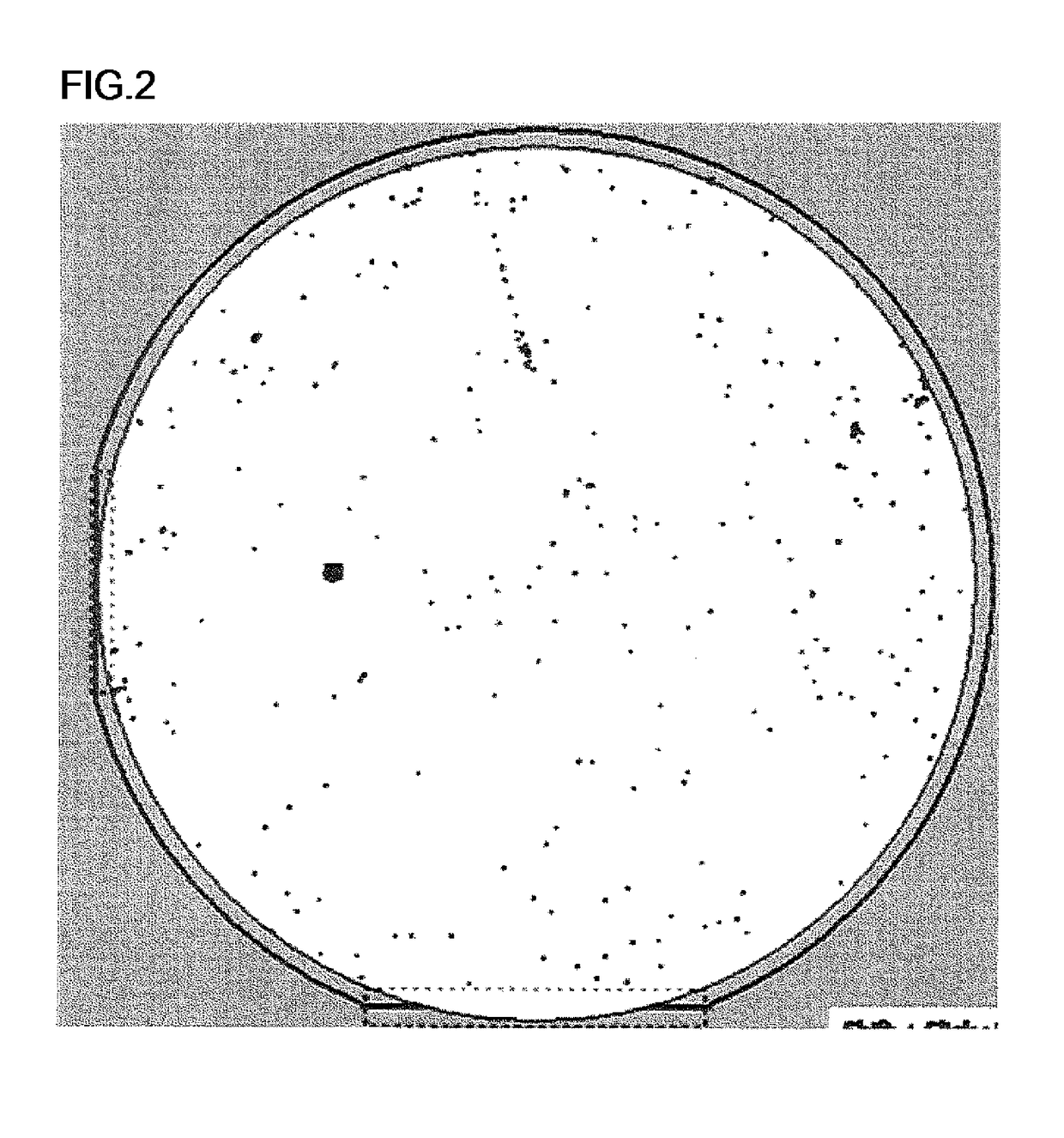
[0060]A surface of a SiC substrate having a polytype of 4H—SiC and an off-angle of 4° was processed by using chemical mechanical polishing, and the arithmetic mean roughness Ra determined by an atomic force microscope. Next a SiC epitaxial film having a 10 μm thickness was deposited by using low pressure CVD, and then the SiC epitaxial film was processed by chemical mechanical polishing to remove a surface portion by 50 nm in depth. Then a defect map was acquired by using a surface defect inspection apparatus with a confocal microscope. In addition, the arithmetic mean roughness Ra was determined for the SiC epitaxial film by using the atomic force microscope.
PUM
| Property | Measurement | Unit |
|---|---|---|
| Temperature | aaaaa | aaaaa |
| Temperature | aaaaa | aaaaa |
| Thickness | aaaaa | aaaaa |
Abstract
Description
Claims
Application Information
 - R&D Engineer
- R&D Manager
- IP Professional
- Industry Leading Data Capabilities
- Powerful AI technology
- Patent DNA Extraction
Browse by: Latest US Patents, China's latest patents, Technical Efficacy Thesaurus, Application Domain, Technology Topic.
© 2024 PatSnap. All rights reserved.Legal|Privacy policy|Modern Slavery Act Transparency Statement|Sitemap