Semiconductor Josephson Junction and a Transmon Qubit Related Thereto

a transmon qubit and magnetic field technology, applied in the field of quantum computing, can solve the problems of introducing sensitivity to charge noise, complex management of magnetic field for interacting qubits, and inconvenient placement of magnets in close proximity of one or more qubits

Active Publication Date: 2017-05-11
UNIVERSITY OF COPENHAGEN
View PDF6 Cites 40 Cited by
  • Summary
  • Abstract
  • Description
  • Claims
  • Application Information

AI Technical Summary

Benefits of technology

[0020]A typical transmon qubit is conventionally configured with a JJ having a SIS configuration. In addition, a typical transmon qubit is also conventionally configured with two JJs, typically in a DC-SQUID configuration. The side gate controlled transmon qubit according to the present invention thus greatly differs from a typical transmon qubit. An effect of the features defined by the side gate controlled transmon qubit according to the present invention is that scaling to many qubits is much simplified. For example, a typical transmon qubit, requiring superconducting current loops, implies first of all that a large current is required, and that complex control electronics must pass into the cryogenic environment through normal coax lines, filters and attenuators. This may be avoided using the present invention. On-chip voltage pulses, i.e. related to tuning a qubit using voltage, are relatively easily screened compared to flux pulses, and will reduce cross-talk between qubit control lines. The main advantage of the present invention is the new ability to control the Josephson energy, and hence the transmon qubit frequency, though depletion of a semiconductor, resembling control of the conductance in a field-effect transistor, thereby linking the new field of quantum computing with well-established semiconductor technology. Tuneable Josephson junctions have been realized and used to construct and realize a side gate controlled transmon qubit which is demonstrated in the examples herein.
[0021]A fifth aspect of the present invention relates to a method for producing a Josephson junction from a hybrid semiconductor superconductor nanostructure.

Problems solved by technology

Several problems are however related to a tuneable qubit, in particular to an external magnetic field as applied in order to tune the qubit.
First of all, an external magnetic field could decrease the ratio of the Josephson energy and the charging energy, thereby introducing sensitivity to charge noise.
Thirdly, it could be inconvenient to place a magnet in close vicinity of one or more qubits.
Finally, it could be complex to manage the magnetic field for interacting qubits.

Method used


Image

  • Semiconductor Josephson Junction and a Transmon Qubit Related Thereto
  • Semiconductor Josephson Junction and a Transmon Qubit Related Thereto
  • Semiconductor Josephson Junction and a Transmon Qubit Related Thereto

Examples


example 1

te Controlled Transmon Qubit

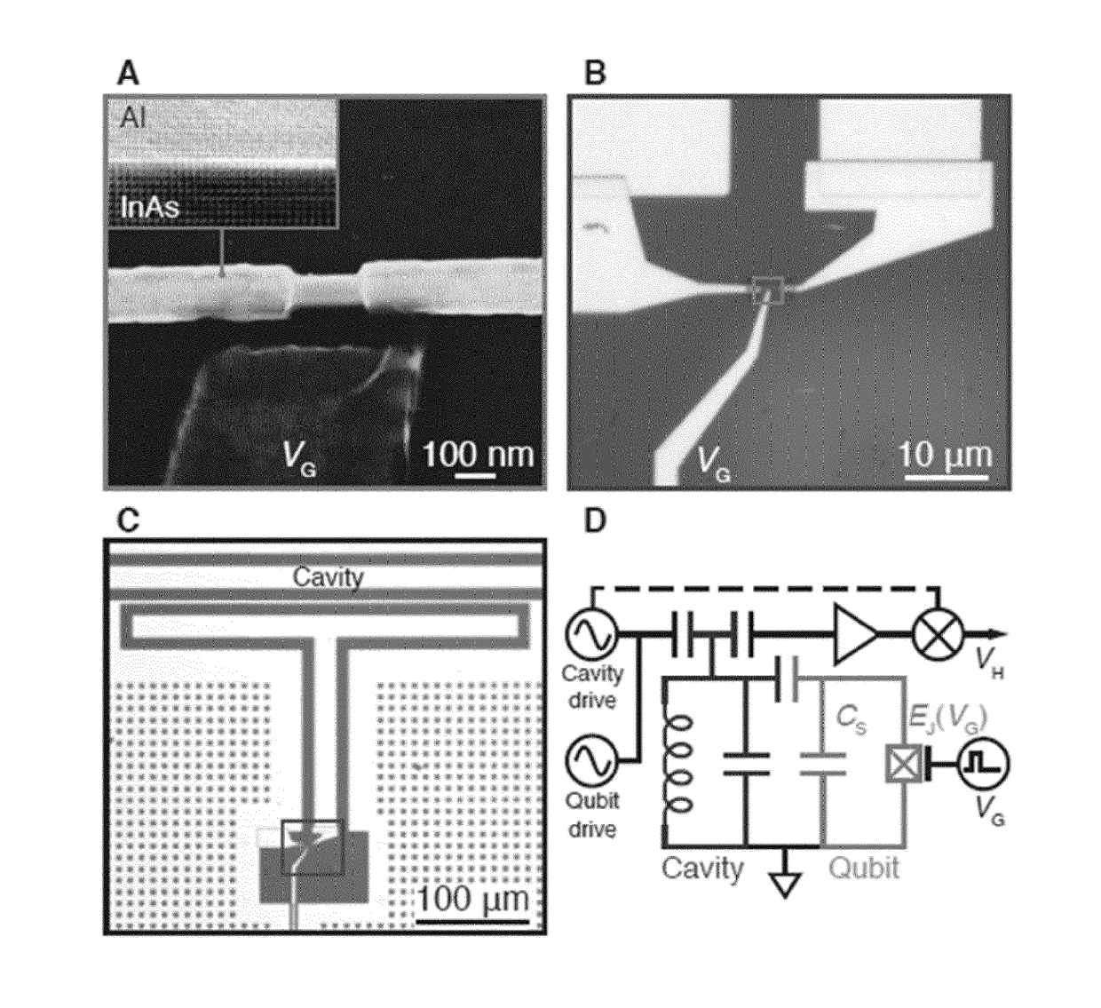
[0106]FIG. 1(A) shows a scanning electron micrograph of hybrid nanostructure in the form of an InAs—Al nanowire with a semiconductor weak link where the Al has been removed forming a Josephson junction. The weak link is formed by wet-etching a segment (˜180 nm) of the epitaxial Al shell. The inset shows a transmission electron micrograph of the epitaxial InAs / Al interface. The epitaxial interface between the superconducting Al the semiconductor InAs is leading to a proximity induced gap in the InAs core with a low density of states below the superconducting gap (a hard gap). The InAs nanowire is formed by MBE growth and is approximately 75 nm in diameter, with an in situ grown ˜30 nm thick Al shell.

[0107]FIG. 1(B-C) show optical micrographs of the completed tunable Josephson junction device according to the present disclosure. The total capacitance of the tunable Josephson junction, i.e. of the side gate controlled transmon qubit, CT, is determined by the...

example 2

upling to a Side Gate Controlled Transmon Qubit

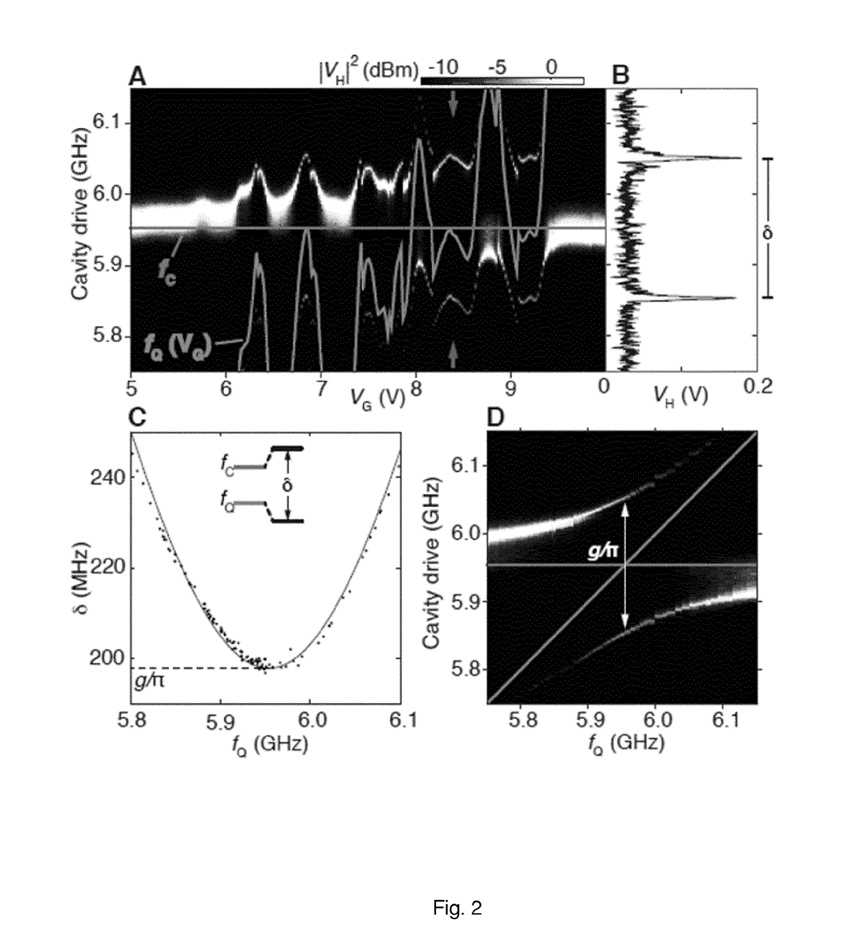
[0109]Side gate controlled transmon cavity coupling is investigated by measuring cavity transmission at low drive power as a function of the cavity drive frequency and gate voltage, VG, with fQ˜fC (FIG. 2(A)). The solid blue line shows the bare cavity resonance frequency, fC, while the solid green line indicates the gate-voltage dependent qubit frequency, fQ(VG), extracted from the data.

[0110]FIG. 2(B) shows cavity transmission as a function of the cavity drive at the position indicated by the purple arrows in (A). Aperiodic fluctuations in the resonance as a function of VG, with regions of widely split transmission peaks, has been observed (FIG. 2B). These gate-dependent, repeatable fluctuations in the cavity resonance are associated with mesoscopic fluctuations in the nanowire transmission appearing also as fluctuations of normal-state conductance, GN(VG) which causes fluctuations in the side gate controlled transmon frequency. The ch...

example 3

Control of a Side Gate Controlled Transmon Qubit

[0113]FIG. 3(A) shows the qubit resonance frequency as a function of gate voltage, VG, and is observed as a distinct feature. Demonstrations of qubit control has been performed in the dispersive regime, fQ−fC>>g / 2π. fQ is obtained by measuring the qubit-state dependent cavity response following a second 2 μs microwave tone. When the qubit drive was on resonance with fQ, a peak in the cavity response was observed, yielding a reproducible gate voltage dependence.

[0114]FIG. 4(B) shows coherent Rabi oscillations performed at point B in (A) (VG=3.4 V) by applying microwave pulse for time, τ, to drive the qubit followed by a readout microwave pulse to probe the cavity response. The main panel shows coherent qubit oscillations as a function of driving frequency and r. The lower panel shows coherent oscillations at the qubit resonant frequency, corresponding to rotations about the X-axis of the Bloch sphere.

[0115]FIG. 4(C) shows coherent oscil...


PUM

PropertyMeasurementUnit
thicknessaaaaaaaaaa
thicknessaaaaaaaaaa
thicknessaaaaaaaaaa

Abstract

The present disclosure relates to semiconductor based Josephson junctions and their applications within the field of quantum computing, in particular a tuneable Josephson junction device has been used to construct a gateable transmon qubit. One embodiment relates to a Josephson junction comprising an elongated hybrid nanostructure comprising superconductor and semiconductor materials and a weak link, wherein the weak link is formed by a semiconductor segment of the elongated hybrid nanostructure wherein the superconductor material has been removed to provide a semiconductor weak link.

Description

CROSS-REFERENCE TO RELATED APPLICATIONS[0001]This application is a U.S. National Stage application of International Application No. PCT / EP2015 / 054522 filed Mar. 4, 2015, which claims priority to EP 14175342.6 filed Jul. 2, 2014 and EP 15154459.0 filed Feb. 10, 2015, the entire contents of each of which are hereby incorporated by reference herein, for all purposes.TECHNICAL FIELD[0002]The present disclosure relates to semiconductor based Josephson junctions and their applications within the field of quantum computing, in particular a tuneable Josephson junction device has been used to construct a gateable transmon qubit.BACKGROUND ART[0003]The fundamental element of a quantum computer is the quantum bit—also known as the “qubit”. As opposed to a classical bit, representing zero and one, a qubit is also able to represent a quantum superposition of the two states. Hence, the states can be formalized within the laws of quantum physics, with a probability. Accordingly, the states can be ...

Claims


Application Information

Patent Timeline
Patent Type & Authority Applications(United States)
IPC IPC(8): H01L39/22H01L39/12H01L39/24H01L39/02
CPCH01L39/223H01L39/025H01L39/125Y10S977/943B82Y10/00Y10S977/81H01L39/2493B82Y40/00H01L29/0673H01L29/413H01L29/437H01L29/66469H10N60/82H10N60/83H10N60/12H10N60/0381Y10S977/762Y10S977/891Y10S977/938H01L29/045H01L29/068C23C14/505C23C14/18C23C14/541C23C14/225H01L29/66977H10N60/01H10N60/128H10N60/80H10N60/11H10N60/805H10N60/855H10N60/0912C23C14/28C30B11/12C30B23/025C30B23/066C30B29/62
Inventor MARCUS, CHARLES M.KROGSTRUP, PETERJESPERSEN, THOMAS SANDNYGARD, JESPERPETERSSON, KARLLARSEN, THORVALDKUEMMETH, FERDINAND
Owner UNIVERSITY OF COPENHAGEN
Why Eureka
Try Eureka