Piezoelectric element, piezoelectric actuator, and electronic apparatus
a piezoelectric actuator and piezoelectric technology, applied in the field of piezoelectric actuators, electronic devices, and piezoelectric elements, can solve the problems of large dielectric loss of disclosed compositions, power consumption and heat generation, and perceived problem of environmental influen
- Summary
- Abstract
- Description
- Claims
- Application Information
AI Technical Summary
Benefits of technology
Problems solved by technology
Method used
Image

Examples
example 1
(Piezoelectric Element)
[0221]The piezoelectric element according to the first mode of the present invention was manufactured.
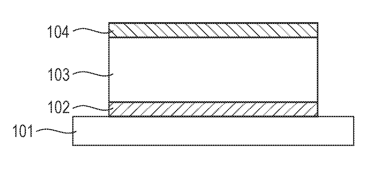
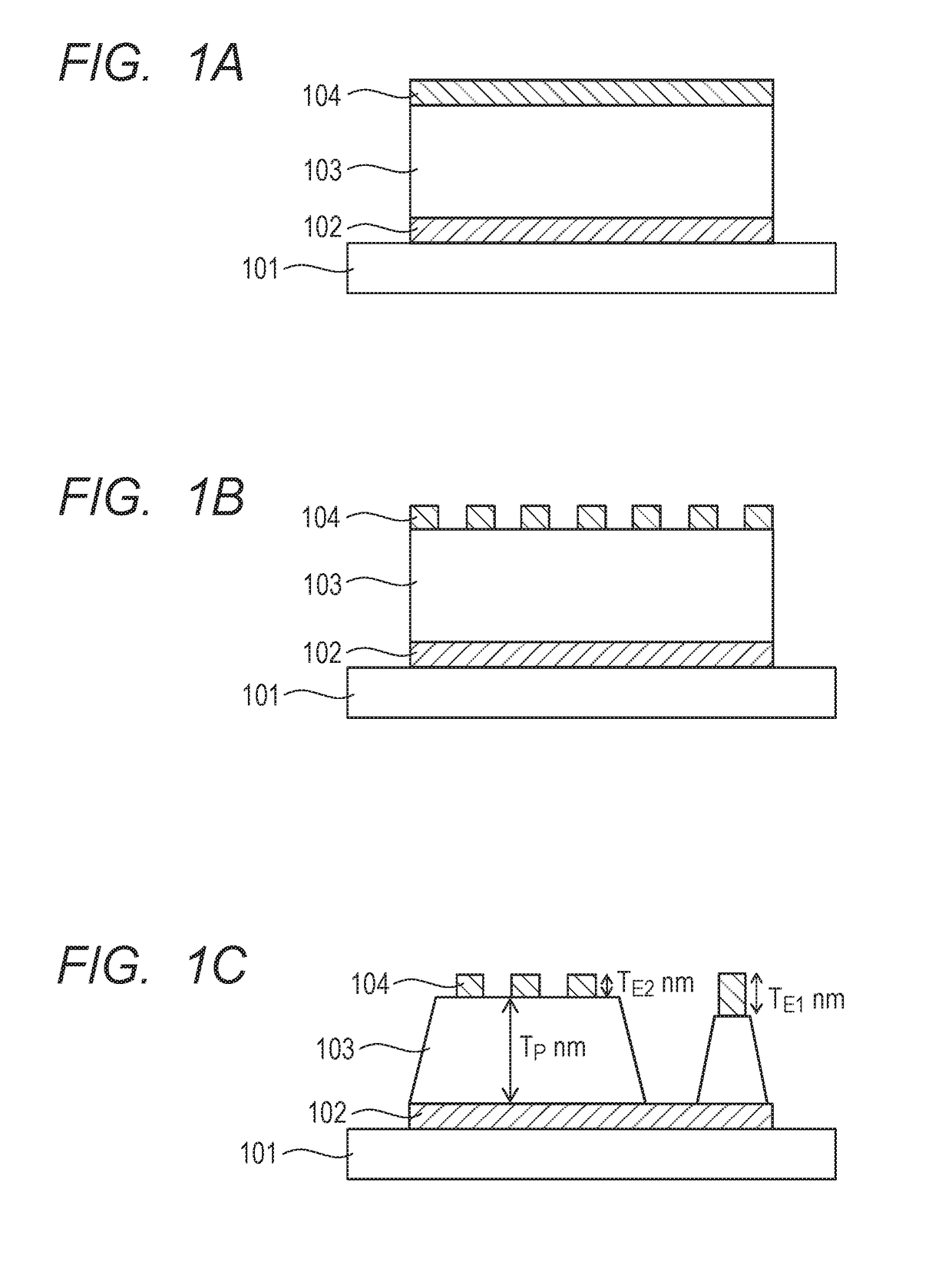
[0222]As the first electrode, a platinum electrode having a thickness of 400 nm was formed on a commercially available silicon substrate by DC sputtering. As an adhering layer, a titanium oxide film having a thickness of 30 nm was formed between the first electrode and the silicon substrate.
[0223]Then, the piezoelectric film containing Ba, Ti, Zr, Mn, and Bi was formed on the first electrode by CSD.
[0224]Specifically, the piezoelectric film containing a material corresponding to a composition Ba(Ti0.960Zr0.040)O3 when x=0.040 in the general formula (1) of Baa (Ti1-xZrx)O3, 0.010 moles of Mn element as the first auxiliary component, and 0.0020 moles of Bi element as the second auxiliary component was manufactured as follows.
[0225]As the precursor material liquid used in application by CSD, one in which alkoxides of the respective metals are mixed and dispersed ...
example 2
[0235]The piezoelectric element according to the first mode of the present invention was manufactured similarly to the case of Example 1, except that the method of manufacturing the piezoelectric film was changed from CSD to RF sputtering.
[0236]For the purpose of using as a target for sputtering, a sintered body corresponding to a target composition of the piezoelectric film was manufactured. However, taking into consideration a difference in evaporation rate in the film formed by sputtering, A-site elements such as Ba and Bi were adapted to be in excess in the target sintered body. Materials for the target were prepared as follows.
[0237]Powdery agents of barium carbonate, bismuth oxide, titanium oxide, zirconium oxide, iron oxide, and manganese dioxide, all of which were at a purity of 99.5% or more and were commercially available, were mixed. At that time, weighing was performed such that Ba, Ti, Zr, Mn, and Bi were at a ratio in composition Ba(Ti0.960Zr0.040)O3+0.010MnO2+0.0020Bi...
examples 3 to 16
[0242]Piezoelectric elements according to the present invention having different compositions were obtained by a manufacturing method similar to those of Example 1 and Example 2. Table 1 shows the composition of the piezoelectric films. Kinds of the substrate, the adhering layer, and the first electrode included in the piezoelectric elements, methods of forming the piezoelectric films, the maximum temperatures in film forming processes, and kinds of the second electrodes are shown in Table 2.
[0243]“(100) oriented monocrystal” of Example 13 in Table 2 refers to a MgO monocrystalline substrate that was cut out such that a film forming surface thereof was a (100) plane. Similarly, in Example 15, a MgO monocrystalline substrate in which a film forming surface was a (110) plane was used, and, in Example 16, a MgO monocrystalline substrate in which a film forming surface thereof was a (111) plane was used.
[0244]Further, “CSD” in the piezoelectric film forming method in Table 2 means that ...
PUM
 Abstract
Description
Claims
Application Information