

Low Temperature High Reliability Alloy for Solder Hierarchy
a high-reliability, low-temperature technology, applied in the direction of soldering apparatus, semiconductor/solid-state device details, manufacturing tools, etc., can solve problems such as damage to printed circuit boards (pcbs) and electronic components
- Summary
- Abstract
- Description
- Claims
- Application Information
AI Technical Summary
Benefits of technology
Problems solved by technology
Method used
Image

Examples
example 1
Alloy A
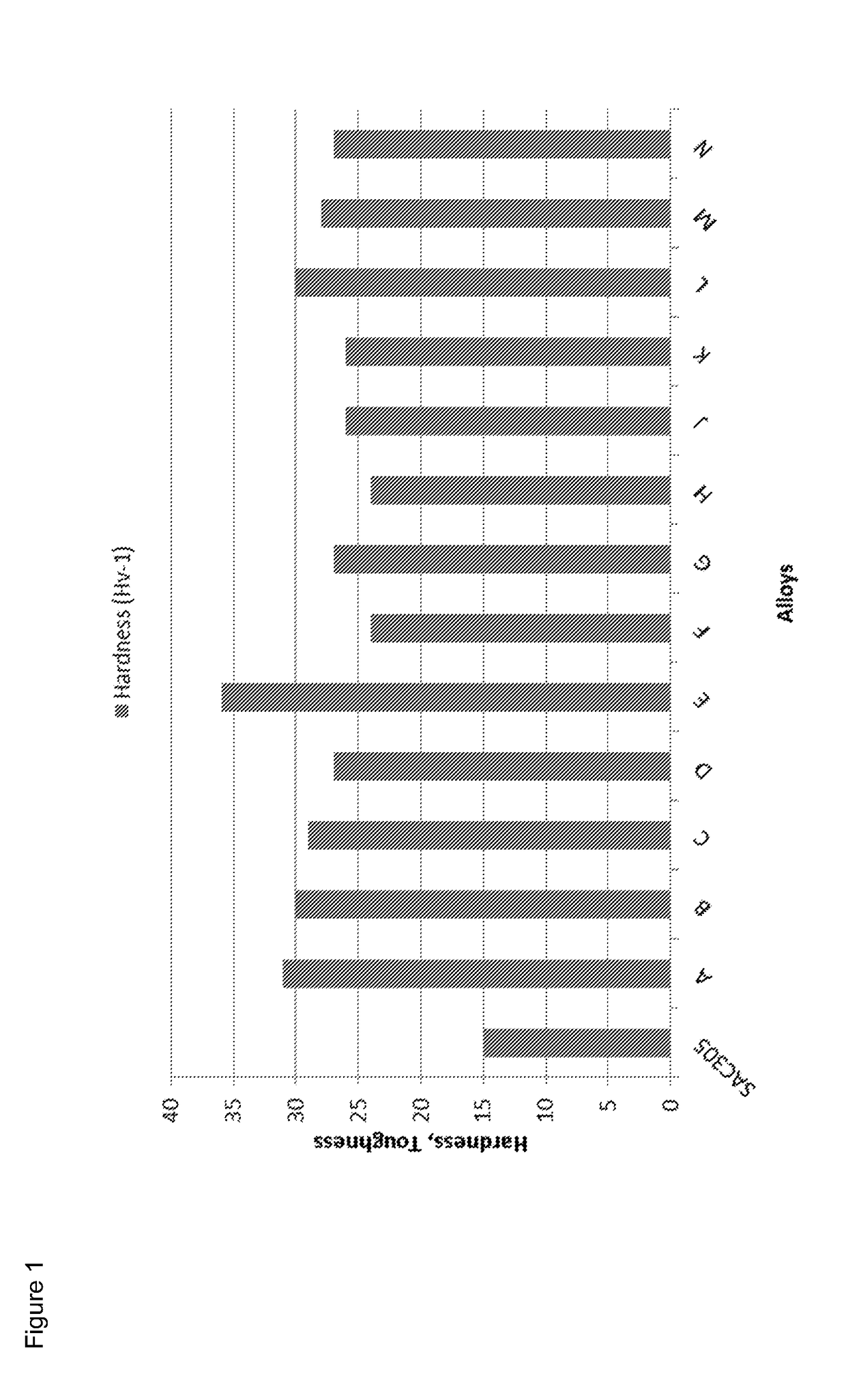
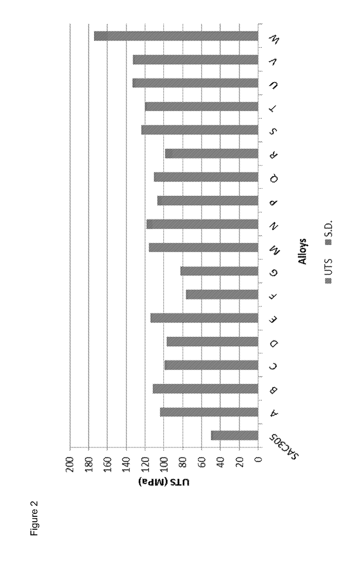
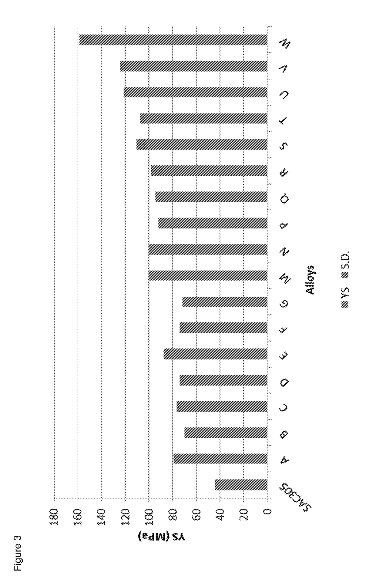
[0257]Alloy A comprises 3.5 wt. % silver, 4 wt. % bismuth, 0.7 wt. % copper, 3.7 wt. % indium, from 0.2 wt. % nickel and the balance tin together with unavoidable impurities. Alloy A has solidus and liquidus temperatures of 196.4 and 209.2° C., respectively, and a Vickers Hardness (Hv-1) of 31. For comparison purposes, the conventional alloy, SnAg3.0Cu0.5, has a melting range of 217.3 to 223.5° C.; and a Vickers Hardness (Hv-0.5) of 15.
[0258]EXAMPLE 2
Alloy B
[0259]Alloy B comprises approximately 3 wt. % silver, 5 wt. % bismuth, 0.7 wt. % copper, 3.75 wt. % indium, 0.1 wt. % nickel and the balance tin together with unavoidable impurities. Alloy B has a melting range of 197.4 and 208.1° C.; and Vickers Hardness (Hy-1) of 30.
example 3
Alloy C
[0260]Alloy C comprises 1.5 wt. % silver, 5 wt. % bismuth, 0.7 wt. % copper, 3.75 wt. % indium, 0.16 wt. % nickel and the balance tin together with unavoidable impurities. Alloy C has a melting range of 191 to 215° C.; and Vickers Hardness (Hy-1) of 29.
example 4
Alloy D
[0261]Alloy D comprises 1.02 wt. % silver, 3.67 wt. % bismuth, 0.68 wt. % copper, 3.5 wt. % indium, 0.12 wt. % nickel , 0.9 wt. % gallium and the balance tin together with unavoidable impurities. Alloy D has a melting range of 190.6 to 212.9° C.; and Vickers Hardness (Hv-1) of 27.
PUM
| Property | Measurement | Unit |
|---|---|---|
| liquidus temperature | aaaaa | aaaaa |
| temperature | aaaaa | aaaaa |
| melting point | aaaaa | aaaaa |
Abstract
Description
Claims
Application Information