Flash Memory

a flash memory and memory cell technology, applied in semiconductor devices, digital storage, instruments, etc., can solve problems such as serious problems, difficult and complex manufacturing processes, and influence on periphery memory cell control circuit transistors or other logic circuit transistors, so as to simplify the optimization of programs, reduce memory cell area, and reduce bit line voltage

Active Publication Date: 2017-08-03
ROBUSTFLASH TECH
View PDF0 Cites 6 Cited by
  • Summary
  • Abstract
  • Description
  • Claims
  • Application Information

AI Technical Summary

Benefits of technology

[0020]Furthermore, as in the fabrication method briefly described in FIGS. 19-22, the etching depth of the surface of a P-well 1 may intentionally tuned in the etching step to form the U-shaped groove. Accordingly, it may be also able to intentionally tune the level difference between the bottom of the multiple insulating film of control gate 5 and the bottom of select gate 7. This tuning may simplify the optimization of program, erase, and read of flash memory.
[0021]Furthermore, the select gate transistor may be able to control punch-through between source and drain by aligning the select gate 7 next to the control gate 5. This may enable channel length across the control gate 5 and the select gate 7 to be shorter, and then reduce memory cell area.
[0022]Furthermore, the

Problems solved by technology

In the conventional technologies, as mentioned above, the process of control gate to be formed later has caused the manufacturing process difficult and c

Method used


Image

  • Flash Memory
  • Flash Memory
  • Flash Memory

Examples


Embodiment Construction

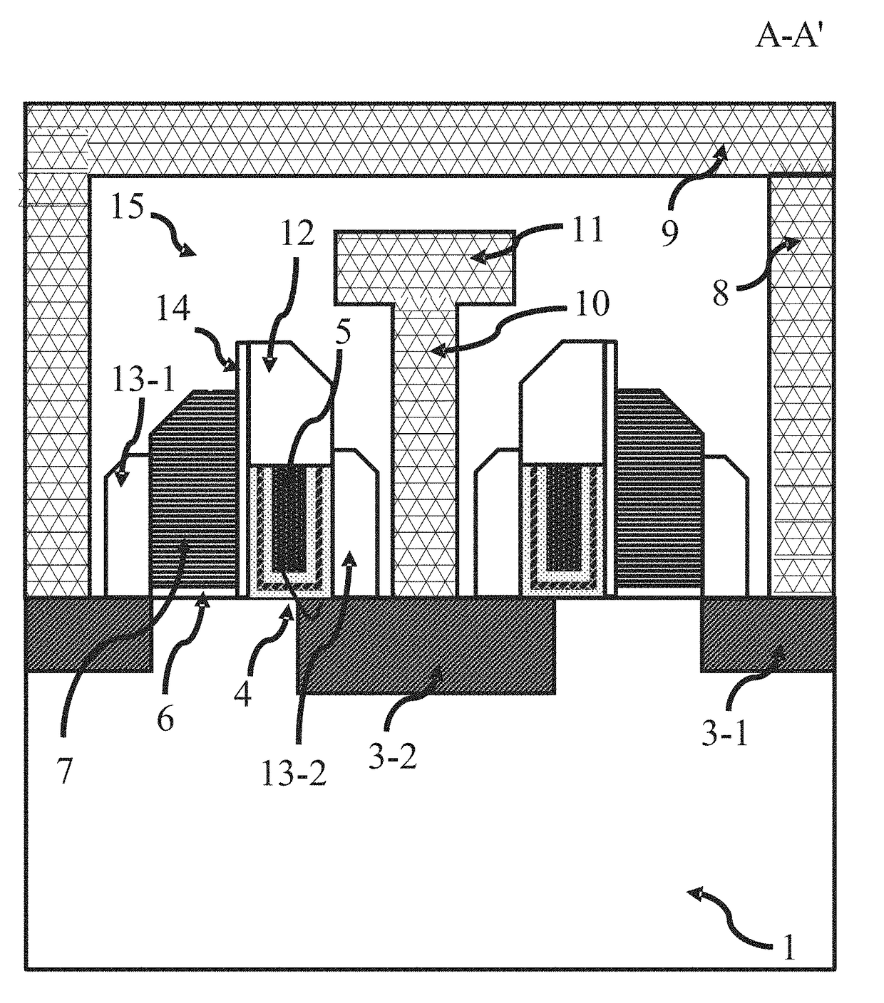
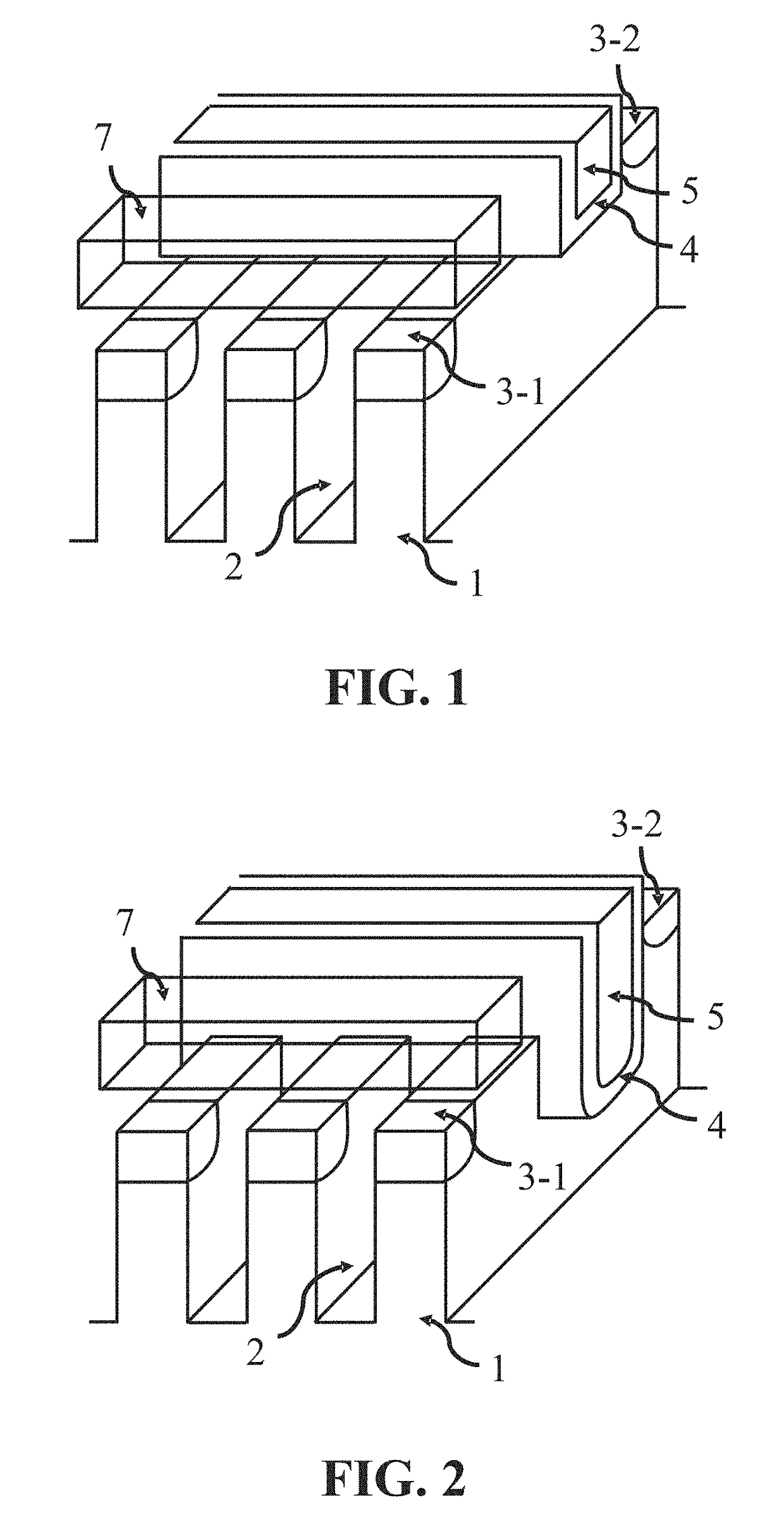
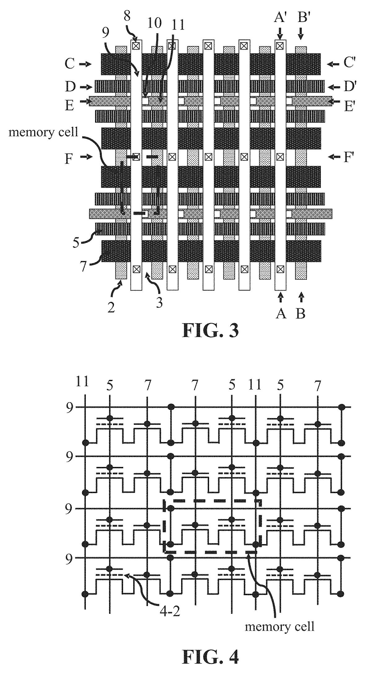
[0048]Hereinafter, the embodiments related to the present disclosure are illustrated with the drawings, wherein similar components or elements are labeled with a same symbol. In addition, the present disclosure is not limited to flash memories, while flash memory is adopted as an example to illustrate the present disclosure. Moreover, the present disclosure is not limited to the embodiments disclosed in the present document.

[0049]FIGS. 1 and 2 are the diagrammatic views of memory cell structure related to the present disclosure. In FIG. 1, a select gate 7 and a control gate 5 lengthen in parallel, and cell isolation regions 2 are formed perpendicular to the select gate 7 and the control gate 5 on the P-well 1 in the memory cell which is isolated from adjoining memory cells along these direction. Moreover, another control gate 5, another select gate 7, and diffusion layers of another source and drain are similarly formed in the region of another memory cell across the cell isolation ...


PUM


Abstract

A cheap and high performance 1.5 transistor-type flash memory highly compatible to external of memory region is provided. The flash memory has sacrifice film formed on substrate. U-shaped groove is formed on sacrifice film, where multiple insulating film is laminated. Multiple insulating film includes silicon nitride film as charge storage layer. Low resistive material is disposed on multiple insulating film to form control gate. Select gate is formed on insulating film on side of control gate in self-aligned manner. Semiconductor regions opposite in conductivity to substrate on both sides of adjoining control gate and select gate to form source and drain, respectively. Thus, a 1.5 transistor-type flash memory is formed with adjoining control gate and select gate between source and drain. In MOS-type transistor with control gate, threshold voltage is changeable according to injection/emission of charge to silicon nitride as charge storage layer, and thus work as non-volatile memory.

Description

CROSS REFERENCE TO RELATED APPLICATIONS[0001]The application claims the benefit of Japan application serial No. 2016-019363, filed on Feb. 3, 2016, and the subject matter of which is incorporated herein by reference.BACKGROUND OF THE INVENTION[0002]1. Field of the Invention[0003]The present disclosure generally relates to the structure of a flash memory, and more particularly, to an electrically erasable and programmable non-volatile semiconductor memory device, and its methods of read, write and erasure.[0004]2. Description of the Related Art[0005]Until we arrive at the present, there are many proposals and practical applications of various NOR-type flash memories. As illustrated in FIG. 16, there are two major types of practical applications. One is floating gate type as a memory cell of flash memory. The other is a type of flash memory, wherein charge is stored in silicon nitride film (SONGS hereinafter). (See Non-Patent Literature 1.) Moreover, the flash memories whose memory ce...

Claims


Application Information

Patent Timeline
IPC IPC(8): H01L27/11568H01L29/423H01L29/51G11C16/04G11C16/14G11C16/26H01L29/16H01L27/11573G11C16/10
CPCH01L27/11573H01L27/11568H01L29/42344H01L29/42348H01L29/513G11C16/10H01L29/4966G11C16/26H01L29/16G11C16/0466G11C16/0483H01L29/495H01L29/4916G11C16/14H10B41/20H10B43/20H10B43/30H10B41/30G11C5/063H01L28/00H10B43/27G11C16/0433H10B43/40
Inventor TSENG, TE-CHANGNAGAI, YUKIHIROSHIROTA, RIICHIROWATANABE, HIROSHI
Owner ROBUSTFLASH TECH
Why Eureka
Try Eureka