Reflective mask blank, method for manufacturing same, reflective mask, method for manufacturing same, and method for manufacturing semiconductor device

a technology of reflective masks and masks, applied in the field of reflective masks, can solve the problems of reducing the precision of the transfer size, reducing the resolution, and leaking exposure light into the adjacent regions, so as to prevent charge-up, reduce the grain size, and high the effect of smoothness

Active Publication Date: 2017-09-14
HOYA CORP
View PDF7 Cites 40 Cited by
  • Summary
  • Abstract
  • Description
  • Claims
  • Application Information

AI Technical Summary

Benefits of technology

[0066]The reflective mask blank according to the present invention includes a conductive underlying film formed on a substrate and adjacent to a multilayer reflective film, the conductive underlying film being made of a tantalum-based material or a ruthenium-based material with a film thickness of greater than or equal to 1 nm, or a laminated conductive underlying film constituted by a tantalum-based material film (layer) made of a tantalum-based material that is formed adjacent to the multilayer reflective film and a conductive film (layer) that is formed between the tantalum-based material film and the substrate. This makes it possible to establish an electrical ground without a circuit pattern formation region being electrically isolated, thereby making it possible to prevent charge-up during a mask pattern defect inspection using electron beams (EB). Therefore, it becomes possible to perform high-sensitivity, high-stable mask pattern EB defect inspections.Here, the tantalum-based material exhibits high dry etching resistance to dry etching processes performed using chlorine-based gases that contain oxygen gas, which are used to etch the multilayer reflective film. When a portion of the multilayer reflective film is etched using a chlorine-based gas that contains oxygen gas to form a light-shielding band, the tantalum-based material undergoes substantially no etching. Therefore, it becomes possible to ensure the conductivity required for the mask pattern EB defect inspection by having the tantalum-based material with the film thickness of greater than or equal to 1 nm.
[0067]Moreover, the film thickness of the tantalum-based material film or the ruthenium-based material in the conductive underlying film or the laminated conductive underlying film is less than or equal to 10 nm. This makes it possible to reduce the grain size and achieve a high degree of smoothness, thereby reducing the number of phase defects in the multilayer reflective film which is formed on top of the conductive underlying film or the laminated conductive underlying film. In addition, this ensures a high degree of surface smoothness of the multilayer reflective film as well, thereby reducing the number of pseudo-defects when the multilayer reflective film is inspected for defects. Also, it becomes possible to perform high-sensitivity defect inspections on the multilayer reflective film. Furthermore, in the case when a tantalum-based material film is used, by setting the film thickness to be less than or equal to 10 nm, the reflectance to out-of-band light in regions such as the light-shielding band or the like in which the tantalum-based material film is exposed after the multilayer reflective film is removed by etching is sufficiently so small that the reflectance does not negatively affect exposure transfer processes.
[0068]The method of manufacturing the reflective mask according to the present invention makes it possible to perform high-sensitivity defect inspections on the mask pattern and on the multilayer reflective film. Also, the incidence of phase defects in the multilayer reflective film is few, thereby making it possible to manufacture a mask that has few defects. Moreover, by using this reflective mask in EUV lithography processes, it becomes possible to provide a method of manufacturing a semiconductor device with few transfer defects.

Problems solved by technology

If this light-shielding band does not make it possible to sufficiently reduce the amount of reflected light, the exposure light leaks into the adjacent regions.
This can cause a decrease in the resolution of the patterns in the adjacent regions or a decrease in the precision of the transfer size, thereby resulting in a reason for a decrease in yield rate.
When the light-shielding band is formed simply using the phase shift film or the absorber film in EUV reflective mask, there is a large amount of reflected light, and this can cause the problems described above.

Method used


Image

  • Reflective mask blank, method for manufacturing same, reflective mask, method for manufacturing same, and method for manufacturing semiconductor device
  • Reflective mask blank, method for manufacturing same, reflective mask, method for manufacturing same, and method for manufacturing semiconductor device
  • Reflective mask blank, method for manufacturing same, reflective mask, method for manufacturing same, and method for manufacturing semiconductor device

Examples


example 1

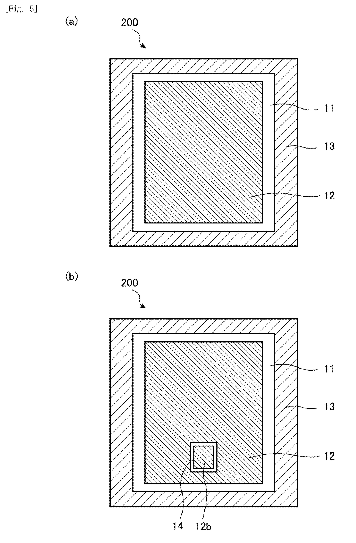
[0138]FIG. 4 shows a series of cross-sectional views schematically illustrating the primary steps in manufacturing an EUV lithography reflective mask 200 from an EUV lithography reflective mask blank 100.

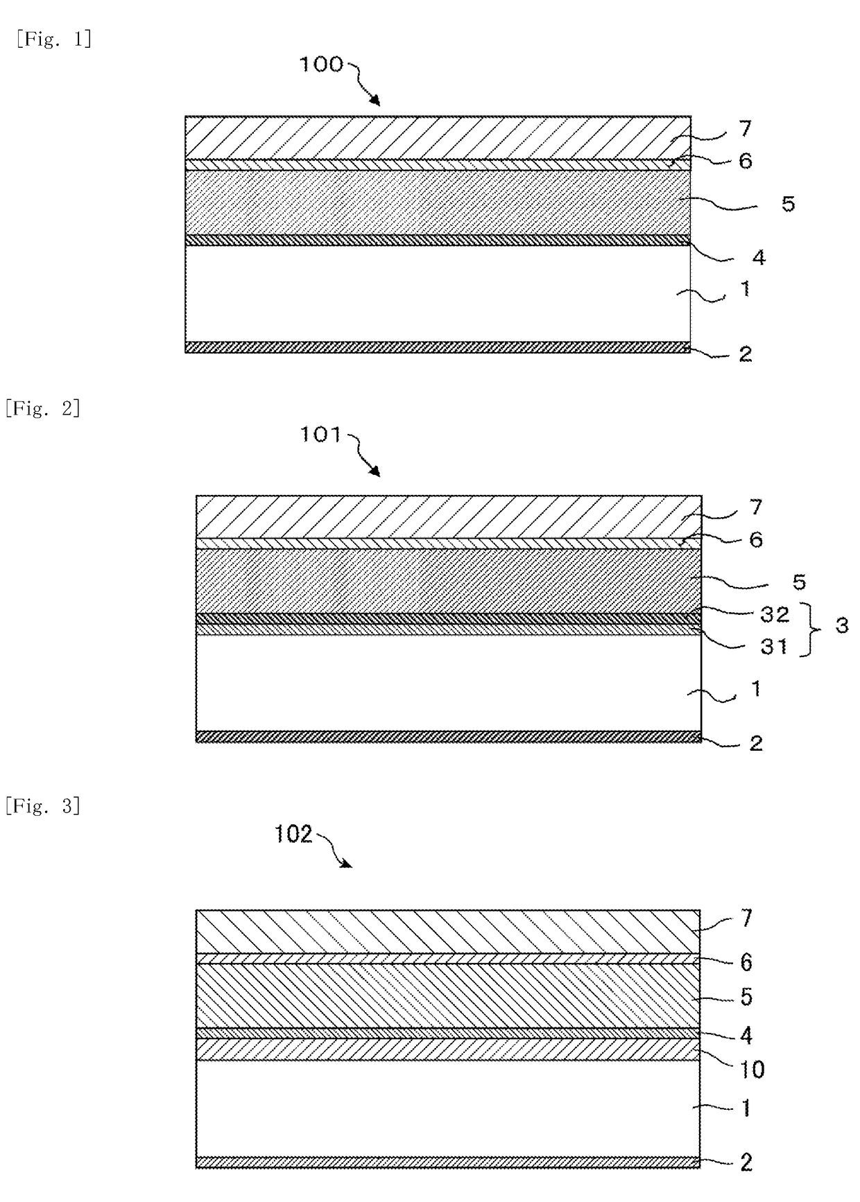
[0139]As illustrated in FIG. 4(a), the reflective mask blank 100 according to Example 1 includes a rear surface conductive film 2, a substrate 1, a single-layer conductive underlying film 4, a multilayer reflective film 5, a protective film 6, and an absorber film 7. Here, the absorber film 7 is a two-layer film that includes a lower absorber film 71 made of TaBN and an upper absorber film 72 made of TaBO. First, the reflective mask blank itself will be described.

Reflective Mask Blank

Substrate

[0140]The substrate 1 was an SiO2—TiO2 low thermal expansion glass substrate having the 6025 size (approximately 152 mm×152 mm×6.35 mm) in which both the first principal surface and the second principal surface were polished. Here, the polishing process included a rough polishing step, a precis...

example 2

[0152]Example 2 is an example of a reflective mask blank in which the material used for the single-layer conductive underlying film 4 was changed from the Ta material used in Example 1 to TaN, the material used for the protective film 6 was changed from the Ru material used in Example 1 to RuTi, and the temperature of the annealing process conducted after the formation of the protective film 6 was changed from 130° C. used in Example 1 to 150° C. The rest of Example 2 was the same as Example 1, including the method of manufacturing the reflective mask and the method of manufacturing the semiconductor device.

[0153]In Example 2, a TaN material (Ta: 90 at. %, N: 10 at. %) with a film thickness of 5 nm was used for the conductive underlying film 4. This film was formed using a DC sputtering process using a Ta target in a mixed gas atmosphere of Ar gas and N2 gas. When the sheet resistance of a sample in which the steps up through the formation of the conductive underlying film 4 were co...

example 3

[0158]In Example 3, a reflective mask blank, a reflective mask, and a semiconductor device were manufactured by using the same configurations and the same methods as in Example 2, except that the order of filming of Si and Mo in the multilayer reflective film 5 was changed so that a Mo film is layered first.

[0159]Accordingly, in a similar manner as Example 2, in Example 3, the multilayer reflective film 5 was formed on the conductive underlying film 4. Here, the multilayer reflective film 5 was a Mo / Si cycle multilayer reflective film including a plurality of Mo and Si layers. By performing an ion beam sputtering process using a Mo target and a Si target in an Ar gas atmosphere, the multilayer reflective film 5 was formed by alternately layering a Mo layer and a Si layer onto the conductive underlying film 4. Here, the Mo and Si sputtering particles were sputtered at an angle of incidence of 30° relative to the normal to the principal surface of the substrate 1. First, a Mo film wit...


PUM

PropertyMeasurementUnit
thicknessaaaaaaaaaa
angle of incidenceaaaaaaaaaa
temperatureaaaaaaaaaa

Abstract

The present invention aims to provide a reflective mask blank and a reflective mask which have a highly smooth multilayer reflective film as well as a low number of defects, and methods of manufacturing the same, and aims to prevent charge-up during a mask defect inspection using electron beams.The present invention provides a reflective mask blank for EUV lithography in which a conductive underlying film, a multilayer reflective film that reflects exposure light, and an absorber film that absorbs exposure light are layered on a substrate, wherein the conductive underlying film is a single-layer film made of a tantalum-based material or a ruthenium-based material with a film thickness of greater than or equal to 1 nm and less than or equal to 10 nm that is formed adjacent to the multilayer reflective film, or the conductive underlying film is a multilayer film including a layer of a tantalum-based material with a film thickness of greater than or equal to 1 nm and less than or equal to 10 nm that is formed adjacent to the multilayer reflective film and a layer of a conductive material that is formed between the layer of the tantalum-based material and the substrate. The present invention also provides a reflective mask manufactured using the reflective mask blank. Furthermore, a semiconductor device is manufactured using the reflective mask.

Description

TECHNICAL FIELD[0001]The present invention relates to a reflective mask blank which is an original plate for manufacturing an exposure mask used to manufacture a semiconductor device or the like, to a method of manufacturing that reflective mask blank, to a reflective mask manufactured using the reflective mask blank, to a method of manufacturing that reflective mask, and to a method of manufacturing a semiconductor device.BACKGROUND ART[0002]The types of light sources used in exposure apparatus for manufacturing semiconductors include g-rays with a wavelength of 436 nm, i-rays with a wavelength of 365 nm, KrF lasers with a wavelength of 248 nm, and ArF lasers with the wavelength of 193 nm, for example. These technologies have evolved to use increasingly shorter wavelengths of light, and extreme ultraviolet (EUV) lithography, which uses extreme ultraviolet (EUV) light with wavelengths near 13.5 nm, has been developed to make it possible to transfer even smaller patterns. In EUV lith...

Claims


Application Information

Patent Timeline
Patent Type & Authority Applications(United States)
IPC IPC(8): H01L21/027C23C14/46C23C14/58C23C14/00C23C14/35G03F1/76C23C14/34G03F1/24G03F1/54G03F1/48G03F1/80G03F7/20C23C14/18C23C14/06
CPCH01L21/0274C23C14/185C23C14/46C23C14/5873C23C14/0036C23C14/35G03F1/76C23C14/3464G03F1/24G03F1/54G03F1/48G03F1/80G03F7/2002C23C14/0641C23C14/34G03F1/86C23C14/18C23C14/5806C23C14/14
Inventor SHOKI, TSUTOMUASAKAWA, TATSUOKOZAKAI, HIROFUMI
Owner HOYA CORP
Why Eureka
Try Eureka