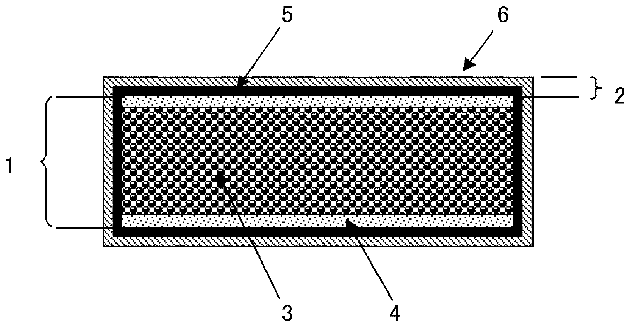
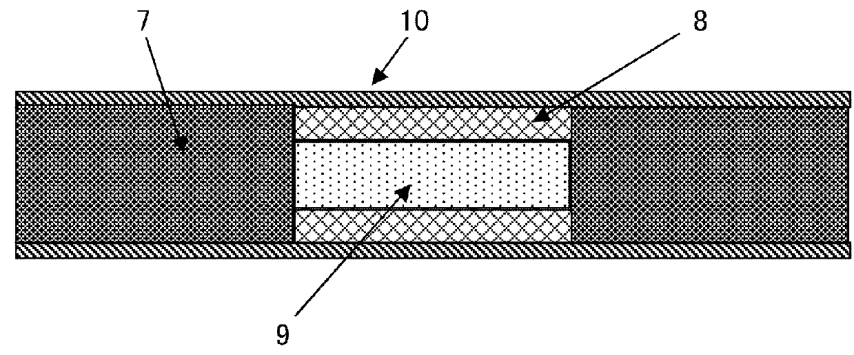
Heat dissipation component for semiconductor element
- Summary
- Abstract
- Description
- Claims
- Application Information
AI Technical Summary
Benefits of technology
Problems solved by technology
Method used
Image

Examples
examples
[0076]In the following, the present invention will be described in more detail, with Examples and Comparative Examples. However, the present invention is not limited to these.
examples 1-13
, Comparative Examples 1-4
[0077]A commercially available high-purity diamond powder A (Diamond Innovations, Inc. / grade MBG600) and high-purity diamond powder B (Diamond Innovations, Inc. / grade MBM) that have average particle diameters shown in Table 1 were mixed at a weight ratio of 7:3. The peak of the volume distribution of the particle diameter of each powder appeared at the same position as the average particle diameter. As a result of the particle size distribution measurement of the mixed powder of the diamond powder A and the diamond powder B, the ratio between the area of the volume distribution at 1-35 μm and the area of the volume distribution at 45-205 μm in the volume distribution was 3:7. In the measurement of the particle size distribution, a slurry was made as a measurement solution, by adding the diamond powders in pure water. Then, the measurement was performed by a spectrophotometer (Beckman Coulter, Inc.: Coulter LS230). The refraction index of the water was 1.33 ...
examples 14-19
, Comparative Examples 5-7
[0088]Ultrasonic cleaning of aluminum-diamond composite bodies made by the same method as Example 1 was performed, and then, pretreatment with the Zn catalyst was performed. Thereafter, a Ni electroplate and an Au electroplate were formed in this order. The thicknesses of the plate films are shown in Table 3. Further, in Comparative Example 7, after the Ni electroplating, a Ni—P electroless plate film was formed.
TABLE 3Plate Film Thickness (μm)Ni ElectroplateNi—P Electroless PlateAu ElectroplateExample140.5—1.5Example151—1.5Example161.5—1.5Example173—1.5Example185—1.5Example196.5—1.5Comparative0.3—1.5Example 5Comparative7.5—1.5Example 6Comparative551.5Example 7
[0089]In Comparative Example 5, a pinhole on the plate film was observed, and the subsequent evaluation was not performed. For the obtained plated products, the peel strength was measured. As a result, in all plated products, the peel strength was 80 N / cm or higher. Furthermore, the obtained plated pr...
PUM
| Property | Measurement | Unit |
|---|---|---|
| Temperature | aaaaa | aaaaa |
| Temperature | aaaaa | aaaaa |
| Length | aaaaa | aaaaa |
Abstract
Description
Claims
Application Information
 - R&D
- Intellectual Property
- Life Sciences
- Materials
- Tech Scout
- Unparalleled Data Quality
- Higher Quality Content
- 60% Fewer Hallucinations
Browse by: Latest US Patents, China's latest patents, Technical Efficacy Thesaurus, Application Domain, Technology Topic, Popular Technical Reports.
© 2025 PatSnap. All rights reserved.Legal|Privacy policy|Modern Slavery Act Transparency Statement|Sitemap|About US| Contact US: help@patsnap.com