System and Method for Temperature Control in Plasma Processing System

a technology of plasma processing and temperature control, applied in the direction of chemical vapor deposition coating, test/measurement of semiconductor/solid-state devices, coatings, etc., can solve the problems of difficult temperature control and non-uniform etching or deposition, and achieve accurate control of temperature distribution and high precision processing

Active Publication Date: 2017-09-28
TOKYO ELECTRON LTD
View PDF9 Cites 13 Cited by
  • Summary
  • Abstract
  • Description
  • Claims
  • Application Information

AI Technical Summary

Benefits of technology

[0004]Temperature control of a substrate being processing within a plasma processing system affects the uniformity of a given plasma process being performed on the substrate. For example, local differences in temperature of the substrate can create local differences in etch rate or deposition rate across the substrate, whic

Problems solved by technology

For example, local differences in temperature of the substrate can create local differences in etch rate or deposition rate across the substrate, which results in non-uniform etching or deposition.
Nevertheless, even with d

Method used


Image

  • System and Method for Temperature Control in Plasma Processing System
  • System and Method for Temperature Control in Plasma Processing System
  • System and Method for Temperature Control in Plasma Processing System

Examples


Embodiment Construction

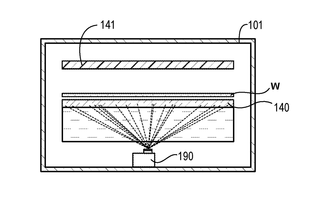
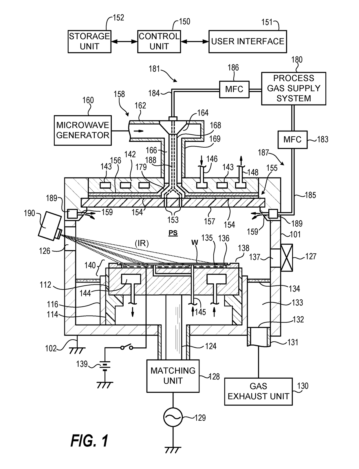
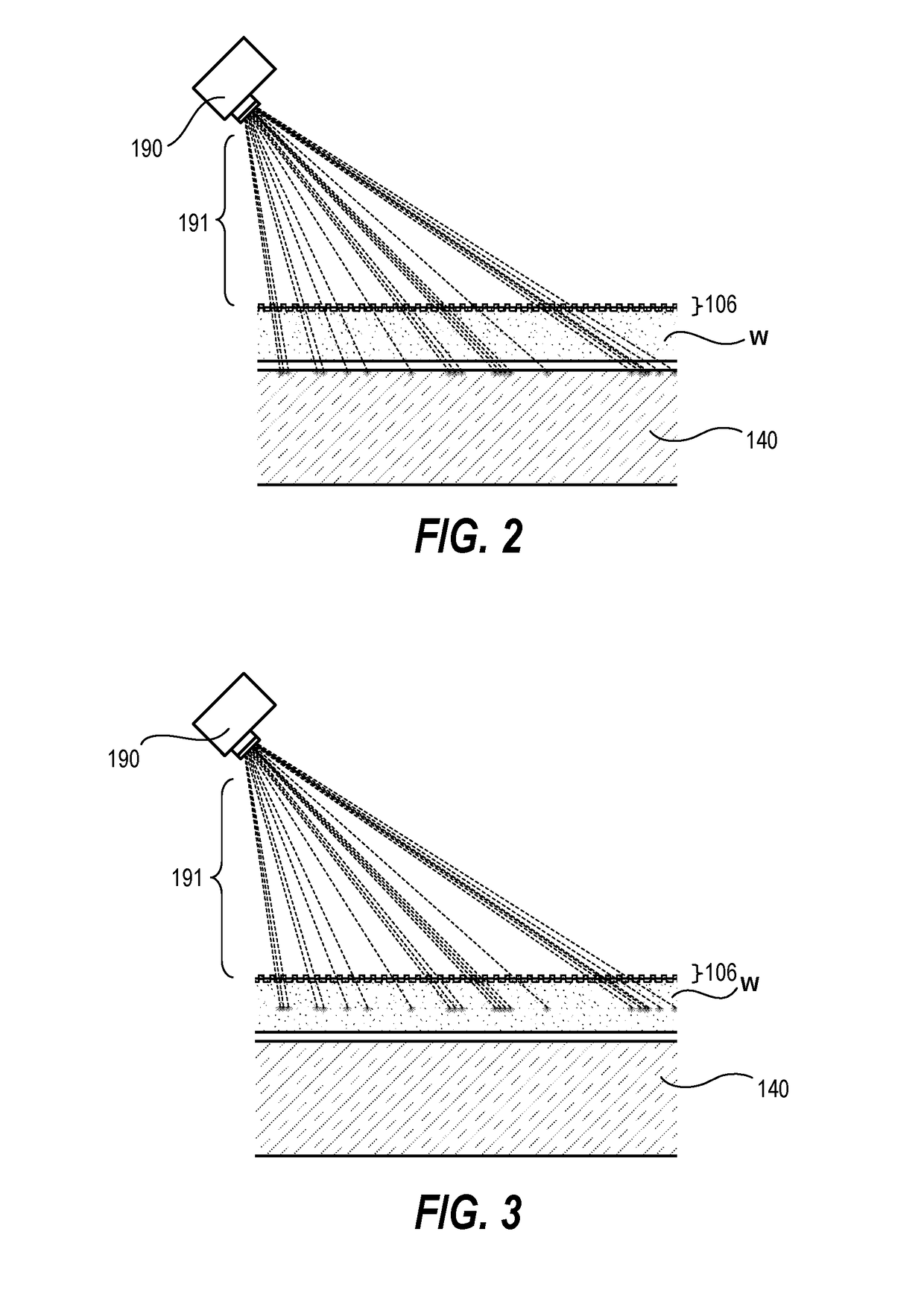
[0022]Techniques herein include systems and methods for fine control of temperature distribution across a substrate. Such techniques can be used to provide uniform spatial temperature distribution, or a biased spatial temperature distribution to improve plasma processing of substrates, such as semiconductor wafers, and / or to correct characteristics of a given substrate. One embodiment includes a plasma processing system with temperature control. Temperature control systems herein include a primary heating mechanism to heat a substrate, and a secondary heating mechanism that precisely modifies spatial temperature distribution across a substrate being processed. This temperature modification can include indirectly modifying substrate temperatures by modifying spatial temperature of a substrate support assembly, or directly modifying an internal temperature or surface temperature of a substrate.

[0023]Referring now to FIG. 1, a schematic cross-sectional view of a microwave plasma proces...


PUM

PropertyMeasurementUnit
Wavelengthaaaaaaaaaa

Abstract

Techniques herein include systems and methods for fine control of temperature distribution across a substrate. Such techniques can be used to provide uniform spatial temperature distribution, or a biased spatial temperature distribution to improve plasma processing of substrates and/or correct characteristics of a given substrate. Embodiments include a plasma processing system with temperature control. Temperature control systems herein include a primary heating mechanism to heat a substrate, and a secondary heating mechanism that precisely modifies spatial temperature distribution across a substrate being processed. At least one heating mechanism includes a digital projection system configured to project a pattern of electromagnetic radiation onto or into a substrate, or through the substrate and onto a substrate support assembly. The digital projection system is configured to spatially and dynamically adjust the pattern of electromagnetic radiation and selectively augment heating of the substrate by each projected point location.

Description

CROSS REFERENCE TO RELATED APPLICATIONS[0001]The present application claims the benefit of U.S. Provisional Patent Application No. 62 / 311,571, filed on Mar. 22, 2016, entitled “System and Method for Temperature Control in Plasma Processing System,” which is incorporated herein by reference in its entirety.BACKGROUND OF THE INVENTION[0002]This disclosure relates to plasma processing systems.[0003]Fabrication of integrated circuits (IC) in the semiconductor industry typically employs plasma processing to create and assist surface chemistry necessary to remove material from and deposit material to a substrate within a plasma processing chamber. Examples of plasma processing apparatus include a plasma CVD (Chemical Vapor Deposition) apparatus configured to deposit a thin film on a substrate, and a plasma etching apparatus configured to remove material from a substrate, which can include using an etch mask to define locations for removing material. In general, such plasma processing appa...

Claims


Application Information

Patent Timeline
IPC IPC(8): H01L21/66C23C16/50H01L21/3065C23C16/46H01L21/683H01L21/67H01J37/32C23C16/458
CPCH01L22/26H01J37/32339H01J37/3244H01J37/32715C23C16/50C23C16/458H01J2237/3321H01L21/6833H01L21/67069H01L21/67103H01L21/3065H01L21/67248H01J2237/334C23C16/46C23C16/047C23C16/481C23C16/511H01J37/32724H01L21/67115C23C16/4586C23C16/48
Inventor DEVILLIERS, ANTON J.
Owner TOKYO ELECTRON LTD
Why Eureka
Try Eureka