Simultaneous Multi-Angle Spectroscopy

a multi-angle spectroscopy and simultaneous technology, applied in the field of metalrology systems and methods, can solve the problems of limiting the throughput of such systems, affecting the measurement effectivity, and loss of signal fidelity, so as to achieve high signal to noise ratio, high throughput, precision and accuracy, the effect of high throughpu

Active Publication Date: 2017-12-14
KLA TENCOR TECH CORP
View PDF2 Cites 6 Cited by
  • Summary
  • Abstract
  • Description
  • Claims
  • Application Information

AI Technical Summary

Benefits of technology

[0010]Methods and systems for performing simultaneous spectroscopic measurements of semiconductor structures over a broad range of angles of incidence, azimuth angles, or both, are presented herein. Spectra including two or more sub-ranges of angles of incidence, azimuth angles, or both, are simultaneously measured over different sensor areas at high throughput with the same alignment conditions. In this manner, machine errors, such as wavelength errors, are uniformly corrected across all measured wavelengths. Collected light is linearly dispersed across different photosensitive areas of one or more detectors according to wavelength for each subrange of AOIs, azimuth angles, or both. Each different photosensitive area is arranged on the one or more detectors to perform a separate spectroscopic measurement of each different range of AOIs, azimuth angles, or both. In this manner, a broad range of AOIs, azimuth angles, or both, are detected with high signal to noise ratio, simultaneously. These features, individually, or in combination, enable high throughput measurements of high aspect ratio structures (e.g., structures having depths of one micrometer or more) with high throughput, precision, and accuracy.
[0012]In this manner, two or more angular segments in the measurement pupil are spatially dispersed such that the measured spectra associated with each angular segment are spatially offset from one another. This allows simultaneous detection by multiple, different detectors, a multiple zone detector, or a combination thereof. In this approach the entire measurement pupil is imaged simultaneously; thus avoiding the limitations of sequential measurements.

Problems solved by technology

This limits the throughput of such system when multiple AOIs are required to accurately characterize the sample.
The resulting loss of signal fidelity limits the effectivity of the measured signals.
Furthermore, time-dependent effects that manifest on the wafer may be captured by the sequential measurements and negatively impact the measurement results.
In summary, ongoing reductions in feature size and increasing depths of structural features impose difficult requirements on optical metrology systems.

Method used


Image

  • Simultaneous Multi-Angle Spectroscopy
  • Simultaneous Multi-Angle Spectroscopy
  • Simultaneous Multi-Angle Spectroscopy

Examples


Embodiment Construction

[0030]Reference will now be made in detail to background examples and some embodiments of the invention, examples of which are illustrated in the accompanying drawings.

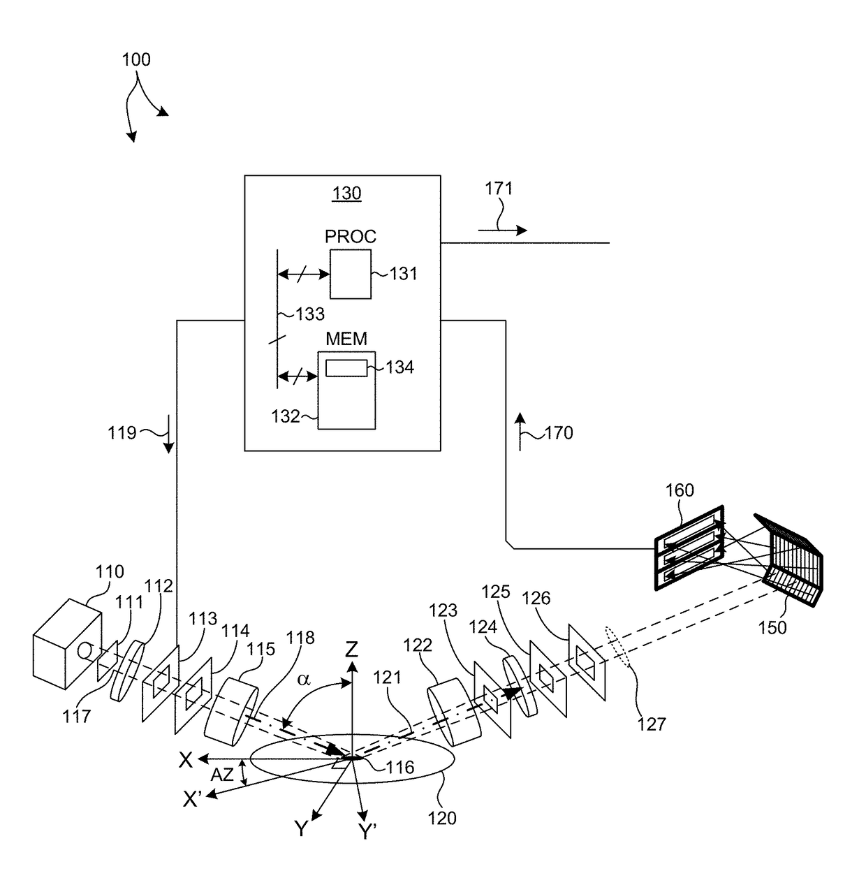
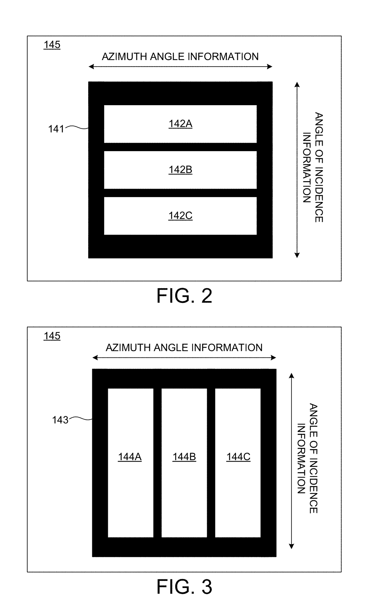
[0031]Methods and systems for performing simultaneous spectroscopic measurements of semiconductor structures over a broad range of angles of incidence, azimuth angles, or both, are presented herein. Spectra including two or more sub-ranges of angles of incidence, azimuth angles, or both, are simultaneously measured over different sensor areas at high throughput with the same alignment conditions. In this manner, machine errors, such as wavelength errors, are uniformly corrected across all measured wavelengths. Collected light is linearly dispersed across different photosensitive areas of one or more detectors according to wavelength for each subrange of AOIs, azimuth angles, or both. Each different photosensitive area is arranged on the one or more detectors to perform a separate spectroscopic measurement of each diff...


PUM

PropertyMeasurementUnit
anglesaaaaaaaaaa
wavelength rangeaaaaaaaaaa
wavelengthsaaaaaaaaaa

Abstract

Methods and systems for performing simultaneous spectroscopic measurements of semiconductor structures over a broad range of angles of incidence (AOI), azimuth angles, or both, are presented herein. Spectra including two or more sub-ranges of angles of incidence, azimuth angles, or both, are simultaneously measured over different sensor areas at high throughput. Collected light is linearly dispersed across different photosensitive areas of one or more detectors according to wavelength for each subrange of AOIs, azimuth angles, or both. Each different photosensitive area is arranged on the one or more detectors to perform a separate spectroscopic measurement for each different range of AOIs, azimuth angles, or both. In this manner, a broad range of AOIs, azimuth angles, or both, are detected with high signal to noise ratio, simultaneously. This approach enables high throughput measurements of high aspect ratio structures with high throughput, precision, and accuracy.

Description

CROSS REFERENCE TO RELATED APPLICATION[0001]The present application for patent claims priority under 35 U.S.C. §119 from U.S. provisional patent application Ser. No. 62 / 348,870, entitled “Optics for Simultaneous Multi-angle Spectroscopy,” filed Jun. 11, 2016, the subject matter of which is incorporated herein by reference in its entirety.TECHNICAL FIELD[0002]The described embodiments relate to metrology systems and methods, and more particularly to methods and systems for improved measurement of semiconductor structures.BACKGROUND INFORMATION[0003]Semiconductor devices such as logic and memory devices are typically fabricated by a sequence of processing steps applied to a specimen. The various features and multiple structural levels of the semiconductor devices are formed by these processing steps. For example, lithography among others is one semiconductor fabrication process that involves generating a pattern on a semiconductor wafer. Additional examples of semiconductor fabricatio...

Claims


Application Information

Patent Timeline
Patent Type & Authority Applications(United States)
IPC IPC(8): G01J3/18G01J3/28G01N21/25G01N33/00G01N21/27G01J3/10G01J3/02
CPCG01J3/189G01N21/255G01N21/27G01N2033/0095G01J3/0289G01J3/10G01N33/00G01J3/2803G01J3/18G01J3/447G01N21/211G01J3/0224G03F7/70633G01N2021/213G01N2021/214G03F7/70616G03F7/70625H01L21/67242H01L22/12H01L22/24H01L22/30
Inventor KRISHNAN, SHANKARBUETTNER, ALEXANDERPURRUCKER, KERSTINWANG, DAVID Y.
Owner KLA TENCOR TECH CORP
Why Eureka
Try Eureka