Infrared spectroscopic reflectometer for measurement of high aspect ratio structures

a spectroscopic reflectometer and high aspect ratio technology, applied in the field of metalrology systems and methods, can solve the problems of many available high-throughput metrology techniques that cannot reliably perform cd and film measurements of high aspect ratio structures, and many optical techniques suffer from low signal-to-noise ratios (snrs), so as to reduce the influence of backside reflection, improve the accuracy of cd and film measurements, and improve the effect of signal-to-noise ratio ratio ratio ratio ratio

Active Publication Date: 2019-02-26
KLA CORP
View PDF49 Cites 2 Cited by
  • Summary
  • Abstract
  • Description
  • Claims
  • Application Information

AI Technical Summary

Benefits of technology

[0011]In another aspect, the spectroscopic measurements are performed off-axis from the direction normal to the surface of the wafer to reduce the influence of backside reflections on the measurement results.
[0012]In yet another aspect, a broad range of infrared wavelengths is detected by a detector that includes multiple photosensitive areas having different sensitivity characteristics. Collected light is linearly dispersed across the surface of the detector according to wavelength. Each different photosensitive area is arranged on the detector to sense a different range of incident wavelengths. In this manner, a broad range of wavelengths are detected with high signal to noise ratio by a single detector. These features, individually, or in combination, enable high throughput measurements of high aspect ratio structures (e.g., structures having depths of one micrometer or more) with high throughput, precision, and accuracy.

Problems solved by technology

Such high aspect ratio structures create challenges for film and CD measurements.
Many optical techniques suffer from low signal-to-noise ratios (SNRs), as only a small fraction of the illumination light is able to reach the bottom of high aspect ratio features, and reflect upwards to the detector.
Thus, many available high-throughput metrology techniques are unable to reliably perform CD and film measurements of high aspect ratio structures.
Cross-sectional scanning electron microscopy (SEM) is a low throughput, destructive technique that is not suitable for inline metrology.
Atomic force microscopy (AFM) is limited in its ability to measure high aspect ratio structures and has relatively low throughput.
CD-SAXS has not yet been demonstrated to achieve high throughput capabilities required by the semiconductor industry.
Model based infrared reflectometry (MBIR) has been used for metrology of high aspect ratio DRAM structures, but the technique lacks the resolution provided by shorter wavelengths and the measurement spot sizes are too large for semiconductor metrology.
Optical CD metrology currently lacks the ability to measure the detailed profile of structures with micron scale depths and lateral dimensions in a relatively small spot (e.g., less than 50 microns, or even more preferably, less than 30 microns) at high throughput.
However, the described techniques suffer from long measurement times for measurements spanning the ultraviolet and infrared wavelengths, wavelength stability limitations, and limited range of infrared wavelengths during operation.
In summary, ongoing reductions in feature size and increasing depths of structural features impose difficult requirements on optical metrology systems.
In this context, speed of broadband illumination and data collection, range of infrared wavelengths have emerged as critical, performance limiting issues in the design of optical metrology systems suitable for high aspect ratio structures.

Method used


Image

  • Infrared spectroscopic reflectometer for measurement of high aspect ratio structures
  • Infrared spectroscopic reflectometer for measurement of high aspect ratio structures
  • Infrared spectroscopic reflectometer for measurement of high aspect ratio structures

Examples


Embodiment Construction

[0033]Reference will now be made in detail to background examples and some embodiments of the invention, examples of which are illustrated in the accompanying drawings.

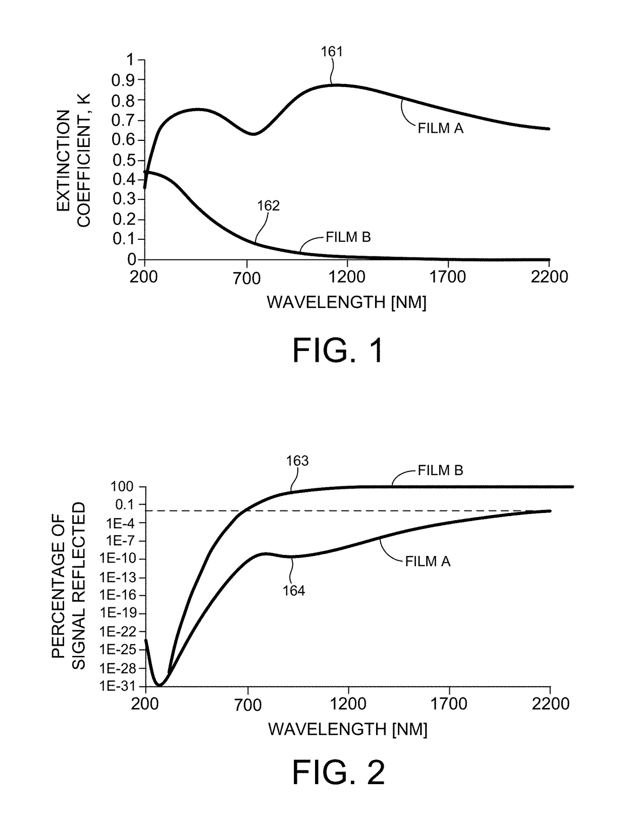
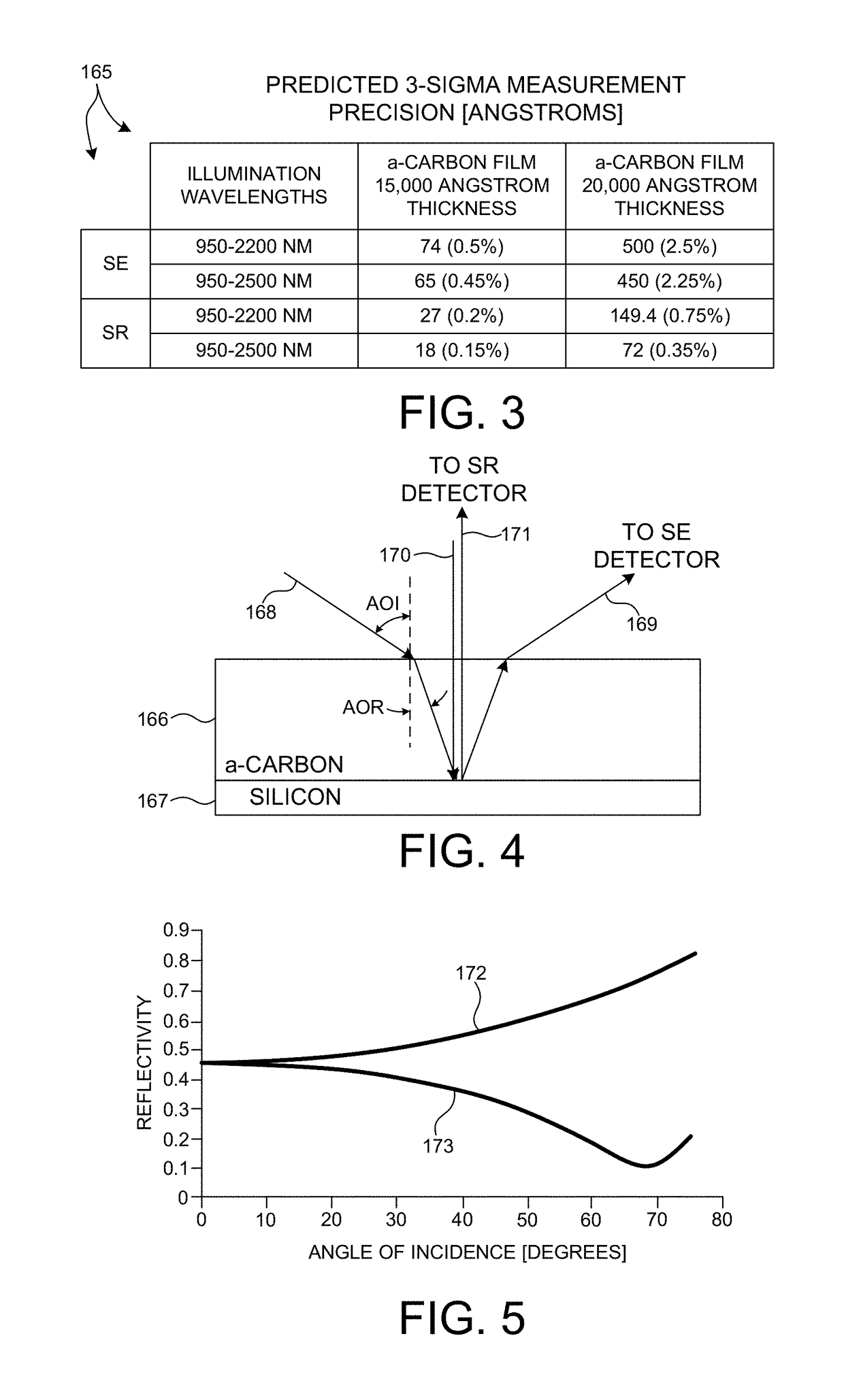
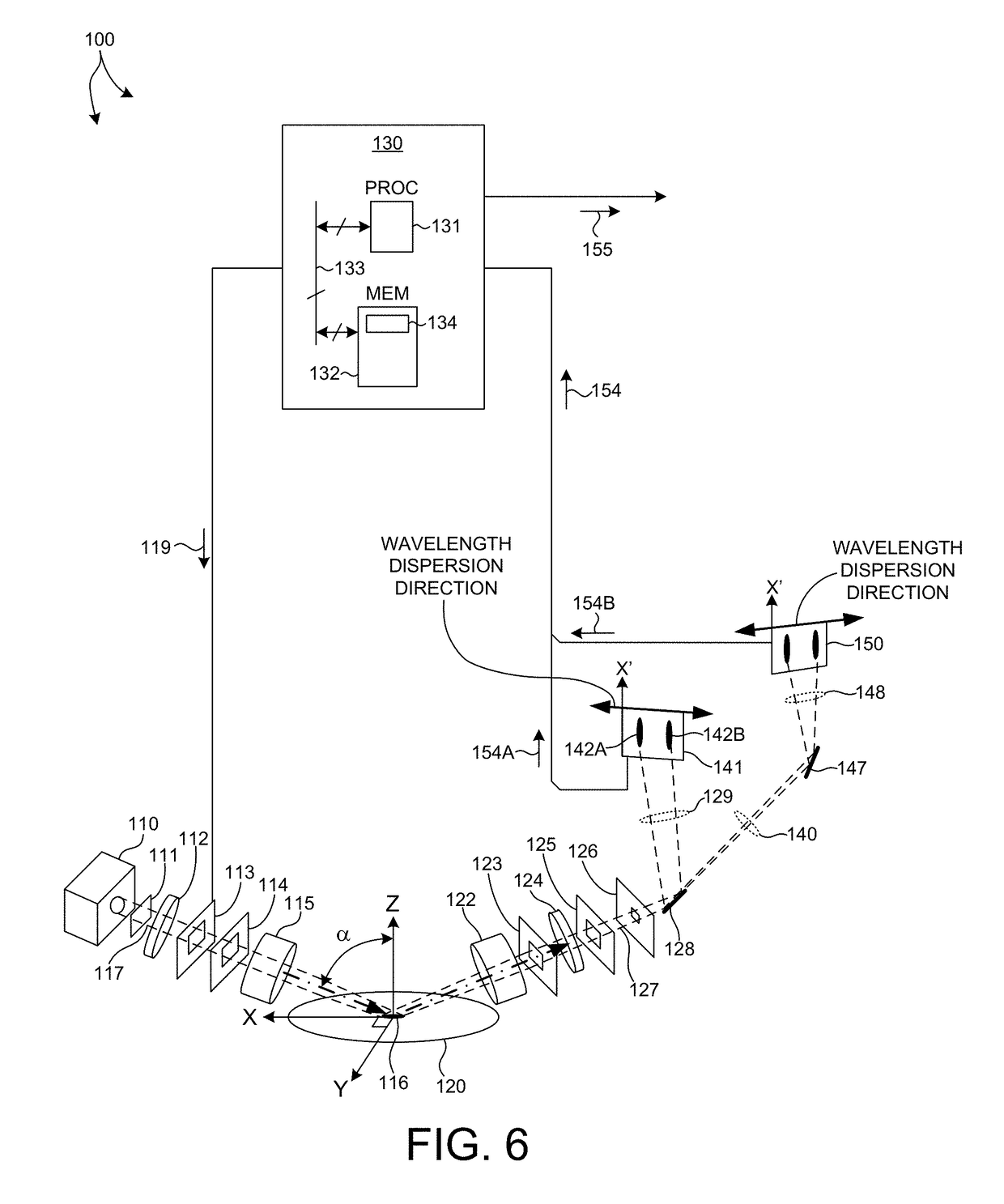
[0034]Methods and systems for performing spectroscopic reflectometry measurements of semiconductor structures at infrared wavelengths are presented herein. In some embodiments, spectra including ultraviolet, visible, and infrared wavelengths are simultaneously measured at high throughput with the same alignment conditions. In this manner, machine errors, such as wavelength errors, are uniformly corrected across all measured wavelengths. In a further aspect, the spectroscopic measurements are performed off-axis from the direction normal to the surface of the wafer to reduce the influence of backside reflections on the measurement results. In another further aspect, a broad range of wavelengths are detected by a detector that includes multiple photosensitive areas having different sensitivity characteristics. Collected ...


PUM

PropertyMeasurementUnit
wavelengthsaaaaaaaaaa
angles of incidenceaaaaaaaaaa

Abstract

Methods and systems for performing spectroscopic reflectometry measurements of semiconductor structures at infrared wavelengths are presented herein. In some embodiments measurement wavelengths spanning a range from 750 nanometers to 2,600 nanometers, or greater, are employed. In one aspect, reflectometry measurements are performed at oblique angles to reduce the influence of backside reflections on measurement results. In another aspect, a broad range of infrared wavelengths are detected by a detector that includes multiple photosensitive areas having different sensitivity characteristics. Collected light is linearly dispersed across the surface of the detector according to wavelength. Each different photosensitive area is arranged on the detector to sense a different range of incident wavelengths. In this manner, a broad range of wavelengths are detected with high signal to noise ratio by a single detector.

Description

CROSS REFERENCE TO RELATED APPLICATION[0001]The present application for patent claims priority under 35 U.S.C. § 119 from U.S. provisional patent application Ser. No. 62 / 401,840, filed Sep. 29, 2016, the subject matter of which is incorporated herein by reference in its entirety.TECHNICAL FIELD[0002]The described embodiments relate to metrology systems and methods, and more particularly to methods and systems for improved measurement of semiconductor structures.BACKGROUND INFORMATION[0003]Semiconductor devices such as logic and memory devices are typically fabricated by a sequence of processing steps applied to a specimen. The various features and multiple structural levels of the semiconductor devices are formed by these processing steps. For example, lithography among others is one semiconductor fabrication process that involves generating a pattern on a semiconductor wafer. Additional examples of semiconductor fabrication processes include, but are not limited to, chemical-mechan...

Claims


Application Information

Patent Timeline
Patent Type & Authority Patents(United States)
IPC IPC(8): G01B11/28G01J3/02G01N21/3563G01J3/28G01N21/55G01B11/00G01N21/47G01N21/33G01N21/21G01N21/31
CPCG01N21/3563G01B11/00G01B11/28G01J3/0229G01J3/2803G01N21/211G01N21/47G01N21/55G01N21/33G01N2021/4711G01N2021/213G01N2021/3137G01N2021/335G01N2021/3568G01B2210/56G01J3/021G01J3/0224G01B9/02G01B11/02
Inventor KRISHNAN, SHANKARWANG, DAVID Y.
Owner KLA CORP
Why Eureka
Try Eureka