Semiconductor Device

a technology of semiconductors and components, applied in the direction of transistors, basic electric elements, electrical equipment, etc., can solve the problems of low current density in the channel, low gate threshold voltage at which the current flow in the channel commences, and complex circuit design including the known transistors

Active Publication Date: 2017-12-28
FRAUNHOFER GESELLSCHAFT ZUR FOERDERUNG DER ANGEWANDTEN FORSCHUNG EV
View PDF8 Cites 6 Cited by
  • Summary
  • Abstract
  • Description
  • Claims
  • Application Information

AI Technical Summary

Benefits of technology

[0011]A back barrier layer is deposited on the substrate or on the optional buffer layer. In some embodiments of the invention, the back barrier layer may contain or consist of AlyGa1-yN. If a separate buffer layer is not present, the back barrier layer may also serve to reduce lattice mismatches between the substrate and subsequent layers. In addition, the back barrier layer may provide an electrical insulation, such that adjacent components are not electrically connected via the substrate.
[0039]In some embodiments of the invention, a metal layer as gate electrode may be arranged on the gate layer. A dielectric intermediate layer may be arranged between the gate electrode and the gate layer. The intermediate layer can increase the gate voltage swing and / or reduce leakage currents between gate electrode and channel.

Problems solved by technology

This known transistor has the disadvantage that the gate threshold voltage at which the current flow in the channel commences is as low as only 200 mV.
This has the effect that circuit design including the known transistor becomes very complex since the gate voltage has to be controlled very accurately.
Furthermore, the known transistor has the disadvantage that the charge carrier concentrations in the conduction band are very low, which results in a low current density in the channel.
However, this known transistor has the disadvantage that the channel is conducting if no gate voltage is present.
This transistor has the disadvantage that complex protective circuits are required in order to avoid destruction of the transistor or of assemblies connected thereto in the case of a fault.

Method used


Image

  • Semiconductor Device
  • Semiconductor Device
  • Semiconductor Device

Examples


second embodiment

[0069]the invention is illustrated with reference to FIG. 5. Like reference numbers designate like parts of the invention, so that the following description is limited to differences between the embodiments shown.

[0070]The second embodiment in accordance with FIG. 5 also uses a back barrier layer 2 having a thickness of 120 nm and an aluminum content of y=0.07. The buried layer 3 arranged thereon has an aluminum content of x=0.12. The dopant concentration is reduced somewhat in comparison with the first embodiment and amounts 3·1017 cm−3. The layer thickness of the buried layer 3 is likewise reduced in comparison with the first embodiment and is approximately 65 Nm.

[0071]A channel layer 4 made from AlGaN having a thickness of 25 nm and an aluminum content of 4% is arranged on the buried layer. A barrier layer 5 is deposited on the channel layer 4, having a thickness of 25 nm and an aluminum content of 26% as described above. A gate layer 6 made from nominally undoped GaN is situated...

third embodiment

[0074]FIG. 7 shows the present invention. For reasons of simplification, the source, drain and gate contacts are not illustrated in FIG. 7. They can be realized in a similar manner than described with respect to the previous embodiments by partly removing the gate layer 6 and providing the free surface regions with corresponding contact elements.

[0075]The third embodiment of the invention is distinguished by the fact that at least one first intermediate layer is arranged between the back barrier layer and the buried layer 3. In the exemplary embodiment illustrated, the first intermediate layer is constructed from a three-layered layer system comprising a first individual layer 31, a second individual layer 32 and a third individual layer 33. In this case, the first and third individual layers comprise AlsGa1-sN and AlTGa1-TN, respectively. The aluminum content S and T of the first intermediate layer 31 and of the third intermediate layer 33 may vary.

[0076]In some embodiments of the ...

fifth embodiment

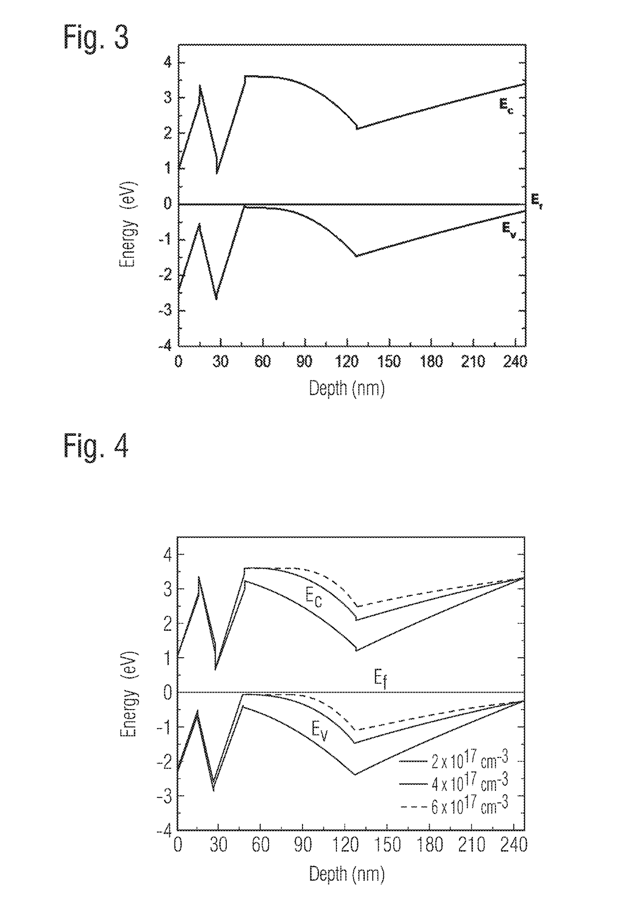
[0086]A calculated band structure of the semiconductor structure according to the invention is illustrated with reference to FIG. 11. As can be seen from FIG. 11, in this case, too, the conduction band minimum is above the Fermi level, such that the semiconductor structure shown in FIG. 10 is likewise suitable for producing a transistor having normally off behavior. The potential well formed by the conduction band is 1.28 eV above the Fermi level, thus resulting in a distinctly positive threshold voltage of the transistor. The potential profile nevertheless enables a good confinement of the two-dimensional electron gas.

[0087]The calculated charge carrier density of the transistor in accordance with the fifth embodiment is 9.5·1012 cm−2

[0088]To summarize, the invention discloses for the first time semiconductor structures which can be used to provide field effect transistors having threshold voltages of more than 0.5 V or more than 0.85 V or more than 1.0 V. The present invention th...


PUM


Abstract

The invention relates to a semiconductor component comprising at least one field effect transistor, said transistor comprising at least a back barrier layer, a buried layer arranged on the back barrier layer, a channel layer arranged on the buried layer, a barrier layer arranged on the channel layer, and a gate layer arranged on the barrier layer, wherein the barrier layer comprises AlzGa1-zN and wherein the buried layer comprises AlxGa1-xN and at least one dopant causing a p-type conductivity, and wherein the gate layer comprises any of GaN and / or AluInvGa1-v-uN. A field effect transistor according to the disclosure may be configured to show a gate threshold voltage which is higher than approximately 0.5 V or higher than approximately 1.0 V.

Description

FIELD OF THE DISCLOSURE[0001]The invention relates to a semiconductor component comprising at least one field effect transistor comprising a back barrier layer, a buried layer arranged on the back barrier layer, a channel layer arranged on the buried layer, a barrier layer arranged on the channel layer, and a gate layer arranged on the barrier layer, wherein the barrier layer comprises or consists of a group-Ill-nitride like AlGaN. Semiconductor components of this type may be used, by way of example, as switching transistors for power electronics.BACKGROUND[0002]It is known from K. Hyeongnam, N. Digbijoy, R. Siddharth and L. Wu: Polarization-Engineered Ga-Face GaN-Based Heterostructures for Normally-Off Heterostructure Field-Effect Transistors; J. of Electronic Materials, Vol. 42, No. 1 2013, to manufacture a field effect transistor comprising five different semiconductor layers deposited one above another. Firstly, a back barrier layer comprising GaN is deposited on a substrate. Th...

Claims


Application Information

Patent Timeline
Patent Type & Authority Applications(United States)
IPC IPC(8): H01L29/778H01L29/417H01L29/207H01L29/10H01L29/205H01L29/20H01L29/423H01L29/34
CPCH01L29/7783H01L29/2003H01L29/205H01L29/207H01L29/34H01L29/41758H01L29/1075H01L29/42316H01L29/432H01L29/201
Inventor BENKHELIFA, FOUAD
Owner FRAUNHOFER GESELLSCHAFT ZUR FOERDERUNG DER ANGEWANDTEN FORSCHUNG EV
Why Eureka
Try Eureka