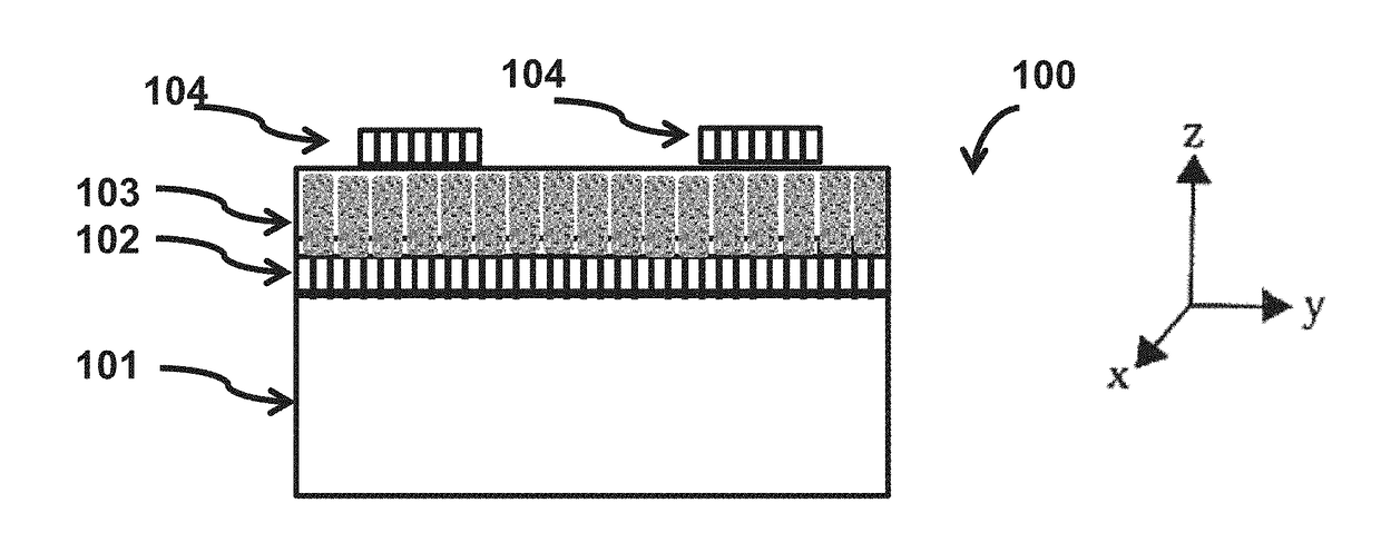
Effect of film defects:
Oxygen vacancies are an inherent defect in both epitaxial and non-epitaxial NLCO films and these defects also introduce strain (bulk strain) into the film.
Specifically,
oxygen vacancies affect nearest neighbor distance by reducing the
Coulomb attractive force between cation and anions in the ionic lattice, resulting in an increased lattice parameter and unit
cell volume, hence introduces film strain.
Furthermore, non-linear thermodynamic models have shown that such
tensile strain results in a minimum of 20% deterioration in the relative
dielectric permittivity of SrTiO3 thin films on Si substrates with respect to its bulk counterpart.
Therefore even though the structural defects are significantly reduced and crystalline grains are grown large in the film during the past-annealing process the films' cannot have desirable dielectric properties exhibiting both high dielectric Q and high dielectric constant / tuning because of
thermal strain in the film.
Thus, the CTE mismatch between the film and the substrate which determines the thermal strains becomes a significant parameter that impacts the films
dielectric response.
Lower annealing temperatures, which impart incomplete film
crystallinity, serves to improve dielectric Q, however the lower
processing temperatures are not effective in elevating the dielectric constant of the film, and as such, the films possess low
permittivity / minimal tunability, hence the ability to promote device
miniaturization is diminished since the size of the tunable device (
resonator, filter, phase shifter etc.) depends on the inverse of the square root of the dielectric constant of the NLCO whereby the larger the dielectric constant the smaller the device component.
Additionally, lower annealing /
processing temperatures lead to smaller grain sizes, which in its lowest limit results in a large
grain boundary area (enhanced leakage path) causing high leakage currents resulting in excessive power draw and often causes premature
voltage breakdown of the film.
The major drawbacks of such substrates are their high cost and small-size-geometry availability ($50-$500+ for ˜1×1-in2·pieces) and they are non-standard to
semiconductor foundry processing industry.
Aside from the direct substrate cost and the limited size availability, the inherent
brittleness of
ceramic substrates, which manifests into
wafer-dicing issues
via device singulation (i.e.,
device breakage), thereby lowering the device yield per substrate, further compromises the device / materials affordability criteria.
Unfortunately achieving such a thick buffer layer film is difficult due to the fact that most films have a
critical thickness after which they become relaxed, hence laden with defects and / or micro-cracks which degrades performance.
Additionally, growth of such thick buffer
layers is not practical from the prospective of extended growth times (e.g., for
sputter deposition on the order of several hours are required to deposit several hundred nanometers of NLCO films, hence significantly longer process times are necessary to deposit microns of film) with its associated elevated cost.
Although fairly successful for simultaneously achieving reasonable Q and high permittivity / wide-tunability, the premise that films were grown on an MgO substrate, which is a non-device relevant substrate material, causes it to be non-compliant with the device affordability and manufacturability requisites.
Finally, this strain mitigation strategy puts forward added processing complexity in that it requires a two-step growth process (buffer layer film+active NLCO film) and this added complexity is undesirable from the
foundry processing point-of-view.
Although this is a successful approach to enable strain relieved SrTiO3 films on device relevant PtSi substrates this method is only useful for solution derived / synthesized thin films, hence this method is fabrication method-limited.
Additionally this approach required long post-deposition annealing times (˜2 hrs. at 750° C.) to impart
crystallinity to the film, such extended annealing schedules translate to longer
foundry times which result in higher manufacturing costs, hence violate the device affordability criteria.
From the prior art summarized herein the mitigation of film strain to achieve a high permittivity and low
dielectric loss (high dielectric Q) NLCO films in concert with other performance, manufacturing and affordability criteria is not easily achieved.

