Ultra-fast method for preparing organic/inorganic thin film by using self-diffusion effects

a thin film, self-diffusion technology, applied in the direction of organic semiconductor devices, sustainable manufacturing/processing, final product manufacturing, etc., can solve the problems of inability to manufacture large area organic solar cells with high efficiency, affecting the commercialization of organic solar cells considered as the next-generation energy source, etc., to achieve the effect of simple process, low material loss, and very rapid and effective formation

Active Publication Date: 2018-07-26
KOREA ADVANCED INST OF SCI & TECH
View PDF6 Cites 4 Cited by
  • Summary
  • Abstract
  • Description
  • Claims
  • Application Information

AI Technical Summary

Benefits of technology

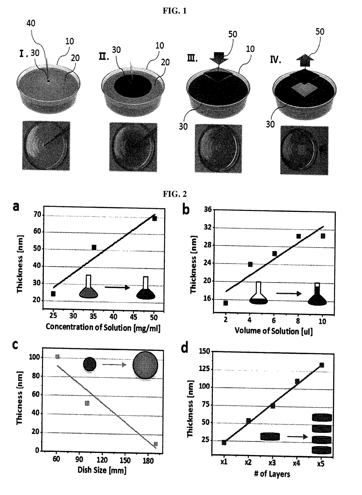
[0022]The present disclosure relates to a method for forming an organic / inorganic thin film on a liquid substrate by using the surface tension between the liquid substrate and a solution and allows for fabrication of an organic / inorganic electronic device including a solar cell, a light-emitting diode, a thin-film transistor, etc.
[0023]According to the present disclosure, a uniform organic / inorganic thin film can be formed very quickly and effectively with little material loss and the process is very simple because the formed thin film can be transferred freely to a glass, plastic or metal substrate without additional treatment.
[0024]In addition, the present disclosure can improve the efficiency of an organic / inorganic electronic device because the nanomorphology of the thin film can be controlled effectively during the crystallization, orientation and phase separation of materials.
[0025]Also, in the present disclosure, the organic / inorganic solution used for spin coating can be utilized without modification. That is to say, the present disclosure solves the problems occurring during thin film formation by the conventional spin coating method that about 90% or more material is lost and it is difficult to attain a uniform thin film because a lot of time is required for optimization due to high sensitivity to such factors as ink composition, interaction between the ink and the surface, etc.
[0026]In addition, the present disclosure allows for effective formation of a multi-layer thin film without limitation to solvent or material. When a multi-layer thin film is formed by the spin coating method, there is a limitation that a solvent which does not dissolves the thin film of the lower layer has to be used. In contrast, according to the present disclosure, a multi-layer thin film can be prepared from various materials because the formed thin film can be transferred freely.
[0027]Whereas the existing thin film formation method such as spin coating is limited in that the process should be conducted under a nitrogen atmosphere because of change in material characteristics due to oxygen or water, the present disclosure can ensure the atmospheric stability of the thin film material because the thin film is formed very quickly. In addition, price competitiveness can be ensured because an organic / inorganic electronic device can be fabricated under an air atmosphere.

Problems solved by technology

Despite the high marketability and applicability, there is an obstacle to the commercialization of the organic solar cell considered as the next-generation energy source due to the difficulties in large-scale process and the R2R (roll-to-roll) process.
Although many researches are being conducted on processes for large-scale process, it is difficult to fabricate large area organic solar cells with high efficiency due to the difficulty in the control of nanomorphology over a large area.
Although the spin coating method has been considered the most effective method for fabricating high-efficiency organic solar cells capable of controlling nanomorphology, it is disadvantageous in that it is inappropriate for commercialization because it is impossible to achieve large-area thin film.
Although large-area thin film can be achieved with many thin film forming methods such as doctor blading, slot-die coating, etc., it is difficult to fabricate high-efficiency organic solar cells due to the difficulty in forming uniform thin films because they are very sensitive to such factors as ink composition, interaction between the ink and the surface, etc.
Although the patent describes that a thin film for a large-area organic solar cell with a flat surface can be prepared by using a spray coating apparatus wherein a feed solution is injected into a center portion and a high-pressure gas is injected around the center portion, it does not solve the problem of significant material loss during the thin film formation through spin coating or remarkably improve the uniformity of the thin film.(Patent Document 1) KR 10-1189172 B

Method used


Image

  • Ultra-fast method for preparing organic/inorganic thin film by using self-diffusion effects
  • Ultra-fast method for preparing organic/inorganic thin film by using self-diffusion effects
  • Ultra-fast method for preparing organic/inorganic thin film by using self-diffusion effects

Examples


example 1

on of Organic Solar Cell Device by Using Spontaneous Spreading Effect I

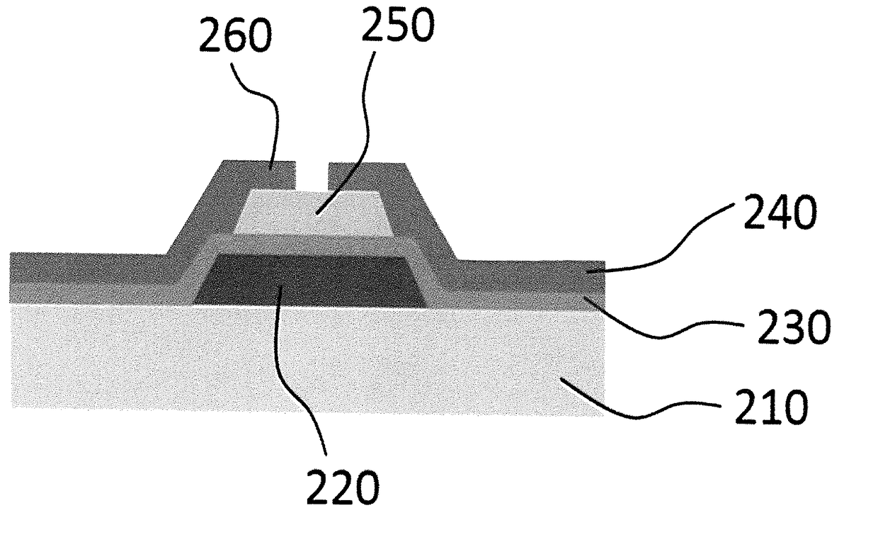
[0070]In this example, an organic solar cell was fabricated in the same manner as in Comparative Example 1, except that 10 μL of a solution prepared by dissolving 15 mg of P3HT and 12 mg of the fullerene derivative PCBM in 1 mL of chlorobenzene was dropped onto distilled water as a liquid substrate and an organic photoactive layer was formed by using the spontaneous spreading effect caused by the difference in surface tension between the two solutions and then transferred onto a hole transport layer.

[0071]The Voc, Jsc and FF of the fabricated organic solar cell were measured to be 0.67, 13.7 and 69%, respectively. The photovoltaic conversion rate was 6.3%. The voltage-current density measurement result is shown in FIG. 6.

example 2

on of Organic Solar Cell Device by Using Spontaneous Spreading Effect II

[0072]An organic solar cell was fabricated in the same manner as in Comparative Example 1, except that ITO having a sheet resistance of 30 Ω / sq and a thickness of ˜1,500 Å was prepared on a PEN substrate, 10 μL of a solution prepared by dissolving 10 mg of PTB7 and 15 mg of PC70BM in 1 mL of a 90:10 (v / v) solvent mixture of chlorobenzene and 1,8-diidooctane (DIO) was dropped onto distilled water as a liquid substrate and an organic photoactive layer was formed by using the spontaneous spreading effect caused by the difference in surface tension between the two solutions and then transferred onto a hole transport layer.

[0073]The Voc, Jsc and FF of the fabricated organic solar cell were measured to be 0.75, 14.7 and 68%, respectively. The photovoltaic conversion rate was 7.3%.

example 3

on of Organic Solar Cell Device by Using Spontaneous Spreading Effect III

[0074]An organic solar cell was fabricated in the same manner as in Comparative Example 1, except that 15 μL of a solution prepared by dissolving 15 mg of PTB7 and 10 mg of the polyperylene derivative PNDI in 1 mL of a 99.5:0.5 (v / v) solvent mixture of chlorobenzene and 1,8-diidooctane (DIO) was dropped onto distilled water as a liquid substrate and an organic photoactive layer was formed by using the spontaneous spreading effect caused by the difference in surface tension between the two solutions and then transferred onto a hole transport layer.

[0075]The Voc, Jsc and FF of the fabricated organic solar cell were measured to be 0.81, 18.8 and 51%, respectively. The photovoltaic conversion rate was 7.7%.


PUM

PropertyMeasurementUnit
diameteraaaaaaaaaa
thicknessaaaaaaaaaa
thicknessaaaaaaaaaa

Abstract

According to the present invention, an ultra-fast method for preparing an organic / inorganic thin film by using self-diffusion effects comprises the steps of: forming a solution by dissolving one or more organic / inorganic materials in a solvent; forming an organic / inorganic thin film by supplying the formed solution onto a liquid substrate; and transferring the formed thin film to a substrate, wherein the step of forming an organic / inorganic thin film forms a thin film on the liquid substrate from the organic / inorganic materials through the occurrence of a self-diffusion phenomenon caused by a difference in surface tension between the liquid substrate and the solution, and through the occurrence of the evaporation of the solvent and the dissolution process of the solvent to the liquid substrate.

Description

TECHNICAL FIELD[0001]The present disclosure provides a method for forming a thin film on a liquid substrate. Specifically, it relates to a method for forming an organic / inorganic thin film through the surface tension between a liquid substrate and a solution by supplying the solution to the liquid substrate.BACKGROUND ART[0002]The fabrication of an organic / inorganic thin film is a fundamental technology in nanotechnology. It is a technology essential for most electronic devices such as mobile phones, military equipment, solar cells, etc., which need to be lightweight, thin and bendable.[0003]Vacuum deposition has been the representative technology for formation of an organic / inorganic thin film since the mid-20th century. There has been a lot of advancement focused on electronic materials and many methods have been proposed. The vacuum deposition techniques include physical deposition and chemical deposition methods. And the wet deposition techniques include electro-plating, spin co...

Claims


Application Information

Patent Timeline
Patent Type & Authority Applications(United States)
IPC IPC(8): H01L51/00H01L51/42H01L51/50H01L51/05H01L51/56
CPCH01L51/0003H01L51/003H01L51/4253H01L51/5012H01L51/0558H01L51/0545H01L51/56H01L51/0096H01L51/0097H01L51/4213H01L51/5056H01L2031/0344H01L51/5024H01L2251/5338H01L51/0036H01L51/0043H01L51/0047H01L51/0035H01L51/0077Y02E10/549B05D1/204Y02P70/50H10K71/12H10K71/80H10K85/215H10K85/113H10K85/701H10K30/30H10K85/50H10K10/466H10K10/484H10K30/10H10K50/11H10K71/00H10K77/10H10K77/111H10K50/12H10K50/15H10K85/30H10K85/111H10K85/151H10K2102/311
Inventor LEE, JUNG YONGJEONG, SEON JUNOH, JONG HYEON
Owner KOREA ADVANCED INST OF SCI & TECH
Why Eureka
Try Eureka