Synthesis and Fabrication of Transition Metal Dichalcogenide Structures

Active Publication Date: 2018-08-09
UNIVERSITY OF SOUTH CAROLINA
View PDF4 Cites 11 Cited by
  • Summary
  • Abstract
  • Description
  • Claims
  • Application Information

AI Technical Summary

Benefits of technology

[0008]According to an embodiment, a method of fabricating a transition metal dichalcogenide (TMD) structure can include first patterning a transition metal (TM) on a substrate and placing the substrate in a process chamber. Instead of using conventional methods of applying various chalcogen sources directly, oxygen can be applied first to the transition metal on the substrate to form transition metal oxides (TMO), which can also be thinned down simultaneously to a desired thickness by sublimati

Problems solved by technology

However, several key obstacles stand in the way of the commercialization of transition metal dichalcogenides (TMDs).
One obstacle in the commercialization of TMD technology is low carrier mobility over large areas for top-down devices

Method used


Image

  • Synthesis and Fabrication of Transition Metal Dichalcogenide Structures
  • Synthesis and Fabrication of Transition Metal Dichalcogenide Structures
  • Synthesis and Fabrication of Transition Metal Dichalcogenide Structures

Examples


Example

Example 1

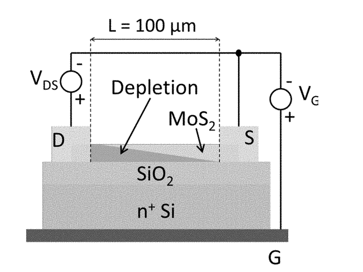
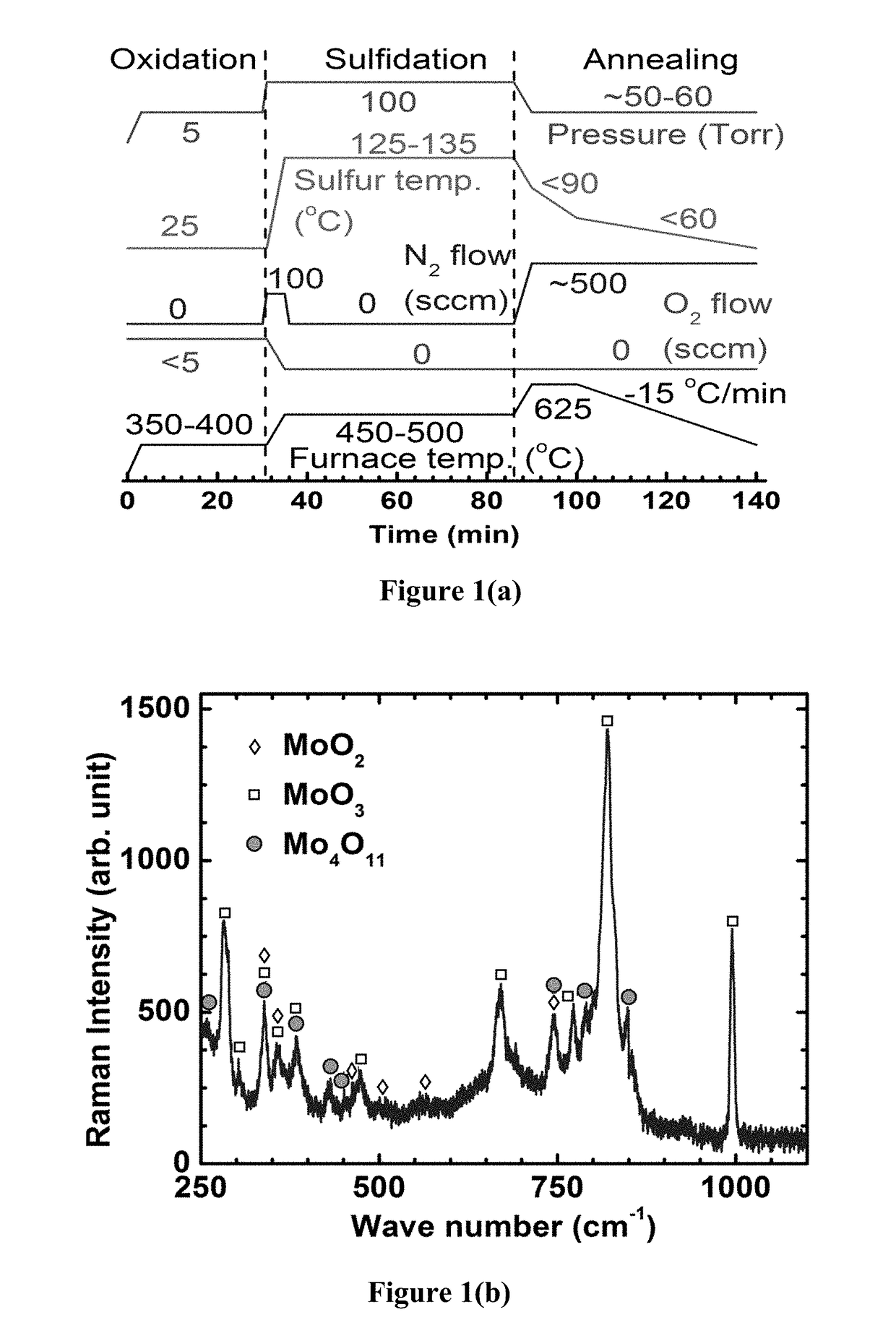
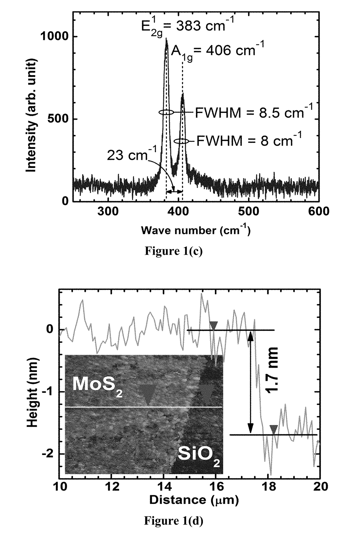
[0059]Top-down growth techniques were utilized for synthesizing large area molybdenum disulfide (MoS2) transistors of a few monolayers in thickness. Patterns of molybdenum were oxidized to form mixtures of volatile molybdenum-oxides and the resulting films were thinned down by partial sublimation at a low temperature. Sulfur vapor was then introduced to the system to sulfidize the volatile oxides to molybdenum disulfide, also at a relatively low temperature (2 with diffused sulfur atoms, which allows the as-grown films to be used without transferring to different substrates, while maintaining high performance transistor characteristics on SiO2 substrates.

[0060]The high quality MoS2 samples were grown on 50 nm SiO2 / n+-Si commercial substrates. A lithographic process was first performed to open up sub-mm sized rectangular windows on a clean SiO2 / Si sample and a layer of molybdenum (Mo) was applied, followed by the electron beam evaporation and lift-off of a 7-10 nm thick laye...

Example

Example 2

[0076]Molybdenum disulfide (MoS2) and other TMDs are analogous to graphene, a two-dimensional layer of carbon atoms in a graphite-like hexagonal lattice. The recent interest in the TMDs stemmed since the discovery of graphene and its exceptional properties, such as extremely high mobility, very high thermal conductivity, surface sensitivity to various molecules, etc. However, graphene based field effect transistors (FETs) perform poorly in terms of switching, owing to its zero band gap. It has been shown by many reports that forming a heterojunction with graphene and another semiconductor can often alleviate this particular problem, while adding a number of other benefits due to the presence of a non-negligible Schottky barrier at the hetero-interface. When the other semiconductor, used with graphene to form the heterojunction, is also a two-dimensional material, there is essentially a 2D heterojunction in place. A key property of these 2D heterojunctions is that each const...

Example

Example 3

[0090]In this example, the graphene / MoS2 barristor from EXAMPLE 2 will be further investigated with a focus on sensing applications of this device. While graphene is inherently sensitive to many chemical species, the sensitivity can be further enhanced by operating a graphene-based device in the exponential (i.e. subthreshold) regime of the transfer curve. This can be achieved conveniently by a barristor device, where a gate bias can be used to tune the barrier height and hence the transport mechanism. Since high barrier height modulation has been shown, it is expected that a high degree of tunability can also be achieved in the sensitivity of the graphene / MoS2 barristor device.

[0091]The sensing experiments were done in a small chamber, which housed the wire-bonded sample. The chamber had an inlet and an outlet. Wires from the device were taken out through a small opening near the outlet, which was stuffed with TEFLON® tape. A roughing pump along with a valve (V3 in FIG. 9)...


PUM


Abstract

Methods of synthesis and fabrication of a transition metal dichalcogenide (TMD) structures are disclosed. A method can include first patterning a transition metal (TM) on a substrate and placing the substrate in a process chamber. Oxygen can be applied to the transition metal on the substrate and a mixture of highly reactive transition metal oxides can be formed and simultaneously thinned down by sublimation. Finally, a chalcogen can be applied to the substrate and a transition metal dichalcogenide structure can be formed.

Description

CROSS-REFERENCE TO RELATED APPLICATION[0001]The present application claims priority to U.S. Provisional Patent Application Ser. No. 62 / 454,298 titled “Asymmetric ambipolar FETs fabricated by large-area, transfer-free growth of a few layer MoS2” of Jahangir, et al. filed on Feb. 3, 2017, the disclosure of which is incorporated by reference herein.GOVERNMENT SUPPORT[0002]The subject invention was made with government support under a research project supported by the National Science Foundation (NSF) grant numbers ECCS-1309466, ECCS-1029346, ECCS-1559711, and CBET 1606882. The government has certain rights in the invention.FIELD OF THE INVENTION[0003]The present disclosure relates to synthesis methods of transition metal dichalcogenide (TMD) for functional structures. More specifically, the present disclosure relates to efficient synthesis methods of TMD materials of very high quality, resulting in structures such as gated and non-gated diodes and transistors, for use in electronic, op...

Claims


Application Information

Patent Timeline
IPC IPC(8): H01L21/02H01L29/78H01L29/24H01L21/324H01L21/263H01L21/768
CPCH01L21/02568H01L29/7839H01L29/24H01L21/02381H01L21/0242H01L21/324H01L21/2636H01L21/02614H01L21/76895H01L21/02488H01L29/66742H01L29/778H01L29/78681H01L29/66969H01L29/7391
Inventor JAHANGIR, IFATKOLEY, GOUTAMCHANDRASHEKHAR, MVS
Owner UNIVERSITY OF SOUTH CAROLINA
Why Eureka
Try Eureka